Method for reducing high concentration doping extension to epitaxial substrate

A high-concentration, substrate technology, used in electrical components, semiconductor/solid-state device manufacturing, circuits, etc., can solve problems such as processing, no silicon nitride film formation process, silicon oxide thickness, etc., to reduce stress and reduce The effect of out-diffusion of impurities

Inactive Publication Date: 2008-01-02
SHANGHAI HUA HONG NEC ELECTRONICS
View PDF0 Cites 1 Cited by
  • Summary
  • Abstract
  • Description
  • Claims
  • Application Information

AI Technical Summary

Problems solved by technology

And the silicon oxide is too thick, the manufacturing cost will be high
[0004] The existing back film layer cannot effectively control the diffusion of impurities in the high-concentration doped substrate
In the high-temperature process, it affects the electrical characteristics of other silicon wafers in the same process. At the same time, because the furnace tube is also diffused by high-concentration impurities, it affects the subsequent products that work in the furnace tube.
[0005] In addition, most of the substrate manufacturing factories do not have a silicon nitride film-forming process, and a single silicon nitride film has a large stress, which may easily cause the substrate to crack or the radius of curvature is too large, making subsequent processing impossible

Method used


Image

  • Method for reducing high concentration doping extension to epitaxial substrate

Examples


specific Embodiment approach

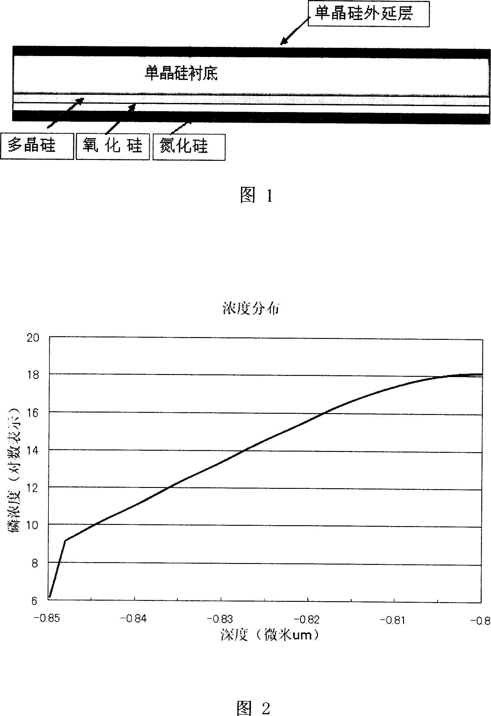
[0019] 1) The substrate is fully cleaned after entering the factory;

[0020] 2) Using low-pressure chemical vapor deposition (CVD) equipment for silicon nitride film growth (500A);

[0021] 3) Scrub both sides of the silicon wafer;

[0022] 4) After entering the dry etching equipment, the silicon nitride on the front side of the silicon wafer is fully etched with carbon tetrafluoride gas;

[0023] 5) After the silicon wafer is fully cleaned, it enters the subsequent processing process.

[0024] Wherein, in step 1), the medicinal solution for cleaning is mainly a combination of diluted hydrogen peroxide+ammonia water and a combination of diluted sulfuric acid+hydrogen peroxide, the purpose of which is to remove organic matter and metal impurities on the surface of the silicon wafer. The interval from step 1) to step 2) is best controlled within 12 hours, otherwise it may affect the cleanliness of the equipment cavity. In step 3), brushing is carried out with a high-pressure...


PUM


Abstract

The invention discloses a method for reducing the disperse of high-density doping material on extent substrate, which adds a silicon nitride film on an extent substrate provided with polysilicon and silicon oxide at back, to reduce the thickness demand of oxide film at back, reduce production cost, reduce the effect on following process, and reduce the outward disperse of high-density doping material.

Description

technical field [0001] The invention relates to a process method for manufacturing a semiconductor device, in particular to a method for reducing the external expansion of high-concentration impurities on an epitaxial substrate. Background technique [0002] Existing power metal oxide semiconductor devices (MOS) use epitaxial substrates, and the concentration of the substrate layer is mostly below 2E19 atoms / cm3. However, with the development of power devices, the requirements for reducing power consumption and reducing the unit transistor area It is getting higher and higher, and the substrate resistance has to be continuously reduced to improve the transistor characteristics. The main method is nothing more than using advanced equipment or other impurities to increase the concentration of impurities. For N-type substrates, red phosphorus (P) will gradually replace arsenic (As) and become the mainstream of N-type impurities, which can increase the doping concentration from...

Claims


Application Information

Patent Timeline
Patent Type & Authority Applications(China)
IPC IPC(8): H01L21/22H01L21/318H01L21/311H01L21/336
Inventor 缪进征龚玲玲
Owner SHANGHAI HUA HONG NEC ELECTRONICS
Why Eureka
Try Eureka