Semiconductor device contact resistant to deterioration due to heat and method for manufacturing contact

一种制造方法、接触件的技术

Inactive Publication Date: 2008-02-06
ALPS ALPINE CO LTD
View PDF0 Cites 4 Cited by
  • Summary
  • Abstract
  • Description
  • Claims
  • Application Information

AI Technical Summary

Problems solved by technology

However, shape memory alloys cannot be formed by plating
Moreover, although a shape memory alloy film can be formed by sputtering a shape memory alloy, if a desired shape is to be obtained by etching after sputtering, the material of the contact member has low etchant resistance to the etchant of the shape memory alloy, so , during the etching of the shape memory alloy, there is a disadvantage that the contacts will also be etched away
In addition, even if the resist is removed (lift-off), the sputtering of the shape memory alloy and its heat treatment must be performed in a high-temperature environment of about 200°C to 500°C, so even if an organic resist material is used Even when patterning is performed, the organic resist material cannot withstand the high-temperature environment, and contacts of the desired shape cannot be obtained.

Method used


Image

  • Semiconductor device contact resistant to deterioration due to heat and method for manufacturing contact
  • Semiconductor device contact resistant to deterioration due to heat and method for manufacturing contact
  • Semiconductor device contact resistant to deterioration due to heat and method for manufacturing contact

Examples


Embodiment Construction

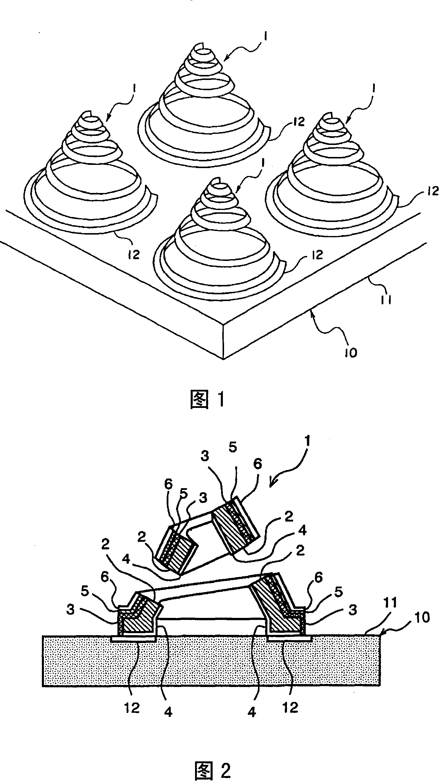
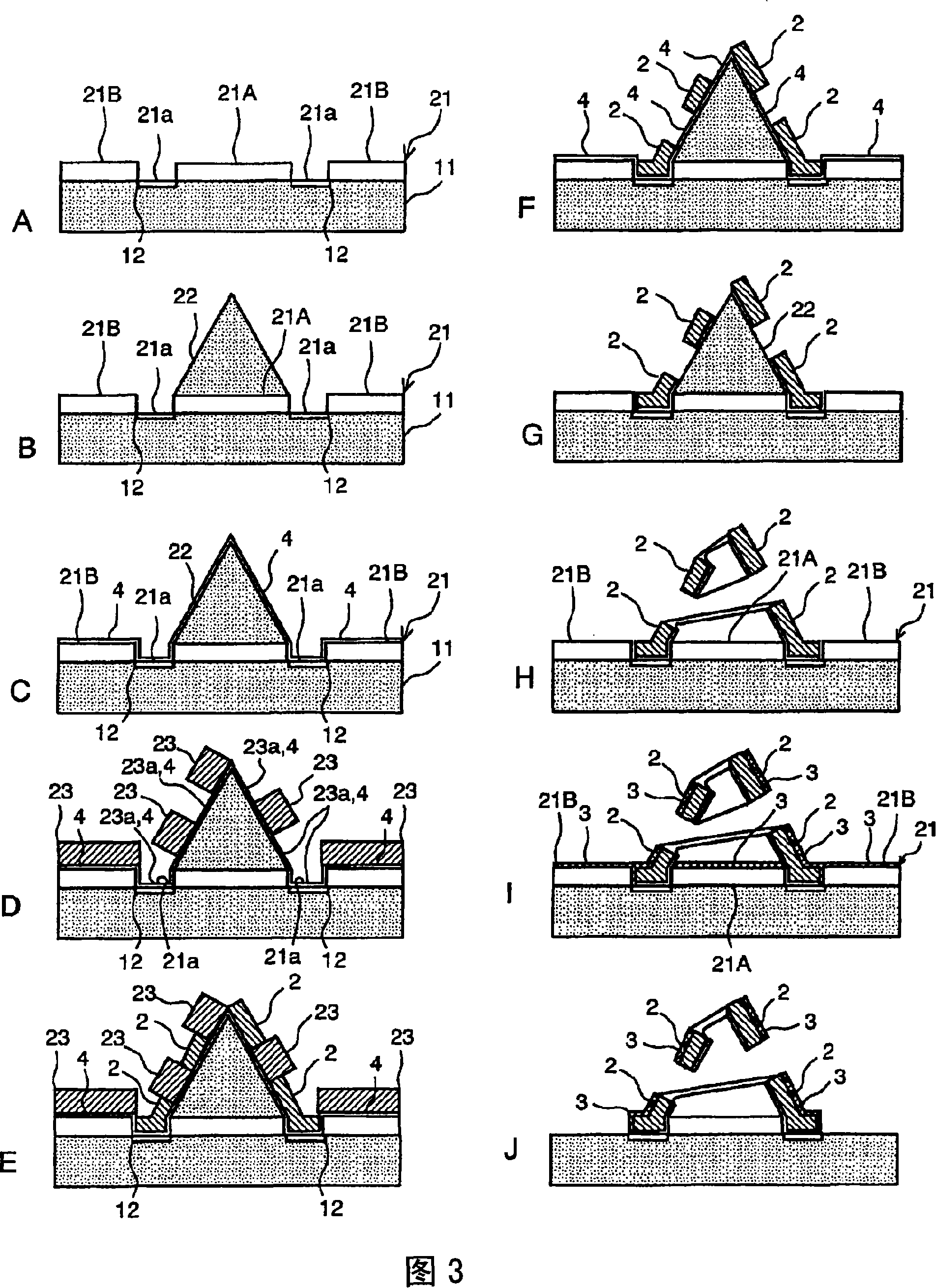
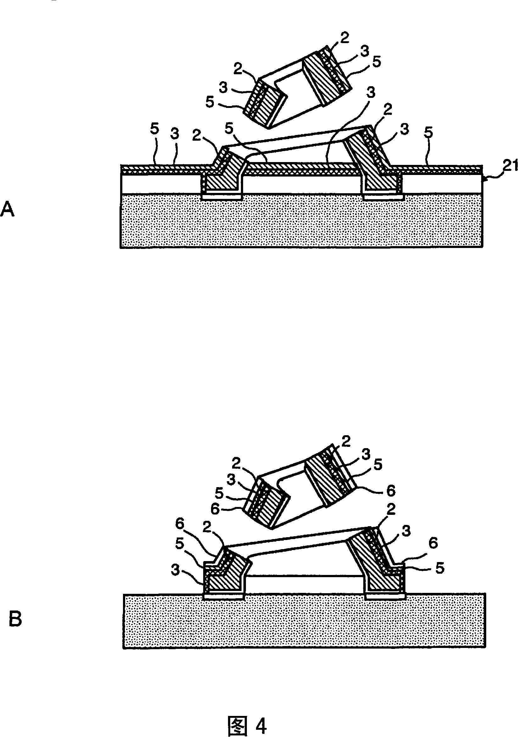
[0049] Next, an embodiment of the contact of the present invention will be described with reference to FIGS. 1 and 2 .

[0050] FIG. 1 is a perspective view showing a contact 1 according to the present embodiment, and FIG. 2 is a vertical cross-sectional view showing the contact 1 according to the present embodiment. As shown in FIG. 1 , the contact 1 of this embodiment is formed in a conical spiral shape with the center as the apex, and is connected to connection terminals 12 formed on an insulating substrate 11 of a probe card (wiring board for inspection) 10 . This contact 1 is formed by laminating a metal spring film 2 and a shape memory alloy film 3 as shown in FIG. 2 . Furthermore, the contact 1 of the present embodiment is formed by laminating the seed film 4 , the conduction auxiliary film 5 , and the conduction film 6 at predetermined positions as auxiliary films for the metal spring film 2 and the shape memory alloy film 3 .

[0051] The metal spring film 2 is forme...


PUM

PropertyMeasurementUnit
martensitic transition temperatureaaaaaaaaaa
diameteraaaaaaaaaa
heightaaaaaaaaaa

Abstract

A Contact according to an aspect of the present invention is formed by laminating a shape memory alloy film on a surface of a metal spring film, and the shape thereof is a conical spiral. A manufacturing method therefor is composed of 11 steps including a step of preparing a sacrificial metal film, a step of forming a resist cone, a step of patterning a resist film, a step of preparing a shape memory alloy film, and the like. Since an organic resist material has poor heat resistance, the sacrificial metal film is formed in advance, the resist is removed before sputtering of the shape memory alloy film, the sacrificial metal film is removed after sputtering of a shape memory alloy and a heat treatment, which are performed at high temperatures, so as to lift off an excess shape memory alloy film.

Description

technical field [0001] The present invention relates to a contact and a manufacturing method thereof, and more particularly to a contact suitable for electrical connection with a semiconductor device having a bump (protruding electrode) formed in a ball shape or a land shape, and to manufacturing the same method. Background technique [0002] Generally speaking, in the manufacturing process of semiconductor devices such as IC (Integrated Circuit: Integrated Circuit) or LSI (Large Scale Integration: IC with an integration level of 1,000 to 10,000 elements), the completed semiconductor device is combined with the so-called As a probe card (probe card) inspection wiring board connection, the input and output of the electrical signal of the semiconductor device can be inspected, thereby reducing the wasteful work caused by assembling defective semiconductor devices into the package (package). [0003] Here, in a probe card for inspecting a BGA (Ball Grid Array: ball grid electr...

Claims


Application Information

Patent Timeline
Patent Type & Authority Applications(China)
IPC IPC(8): H01R13/24H01R43/16H01R33/76
CPCG01R1/06733H01R13/03H01L2924/01004H01L2924/01079H01L2924/01025H01L24/72H01L2224/16H01L2924/14H01L2924/01019H01R12/57H01L2924/00013H01R12/718H01L2924/01078H01R13/2421H01R4/01G01R31/2863H05K7/1069G01R1/06755H01L2224/13099H01L2224/13599H01L2224/05599H01L2224/05099H01L2224/29099H01L2224/29599
Inventor 村田真司
Owner ALPS ALPINE CO LTD
Why Eureka
Try Eureka