Optical waveguide and its manufacture method thereof

A manufacturing method and optical waveguide technology, which is applied in the field of optoelectronic communication, can solve the problems of limited optical signal loss reduction, long manufacturing process, etc., and achieve the effects of reducing diffuse reflection, simple manufacturing process, and reducing production costs

Active Publication Date: 2008-02-13
CHINA WAFER LEVEL CSP
View PDF0 Cites 26 Cited by
  • Summary
  • Abstract
  • Description
  • Claims
  • Application Information

AI Technical Summary

Problems solved by technology

This method also has its disadvantages, first of all, the process of manufacturing process is relatively long
After the soft mold is covered and then removed, it is easy to produce residues
In addition, the more serious problem is the mirror surface. The soft mold can only use the optical fiber material itself to make the mirror surface. The reflection effect of the mirror surface is limited by the material, which limits the reduction of optical signal loss.

Method used


Image

  • Optical waveguide and its manufacture method thereof
  • Optical waveguide and its manufacture method thereof
  • Optical waveguide and its manufacture method thereof

Examples


Embodiment Construction

[0058] In the following description, numerous specific details are set forth in order to provide a thorough understanding of the present invention. However, the present invention can be implemented in many ways other than those described here, and those skilled in the art can make similar extensions without departing from the connotation of the present invention. Accordingly, the invention is not limited to the specific implementations disclosed below.

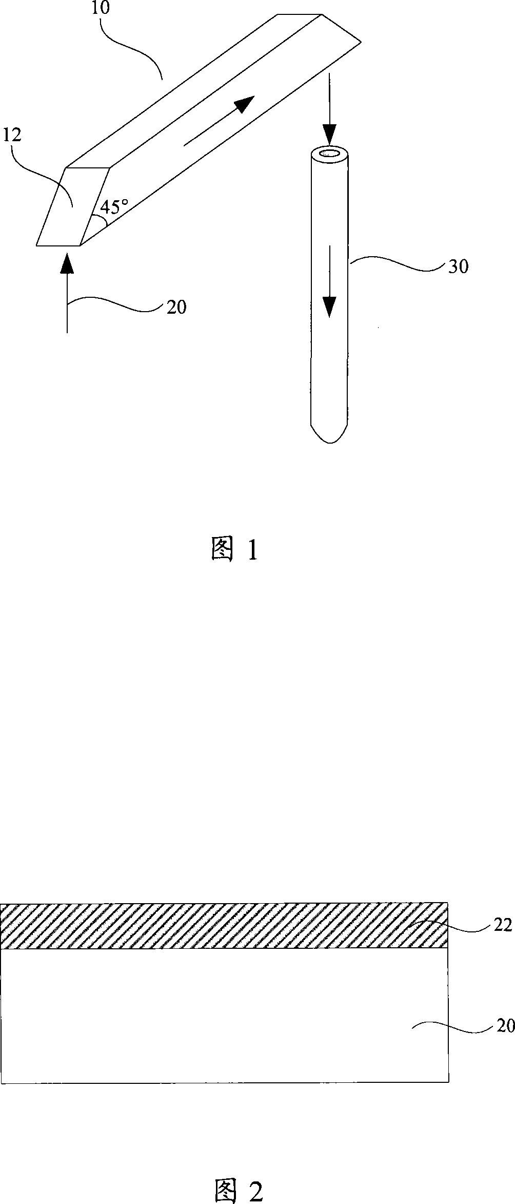
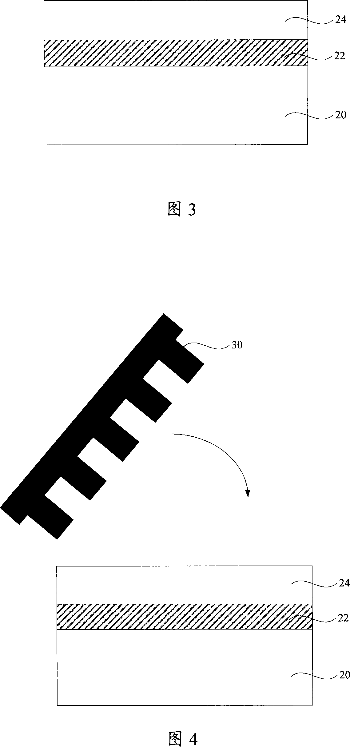
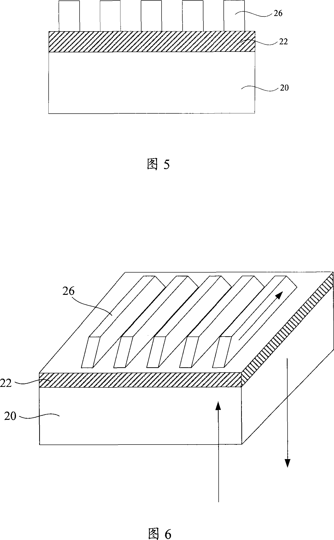
[0059] The method for manufacturing an optical waveguide according to an embodiment of the present invention includes the following steps: firstly, a substrate is provided; a confinement layer is formed on the substrate, and grooves are formed in the confinement layer, and the end surfaces on both sides of the groove are inclined surfaces; at least A metal layer is formed on the surface of the inclined plane; at least a core layer is formed by spin coating in the groove; and a first cladding layer is formed by spin coating bef...


PUM


Abstract

The invention provides a wafer-level optical waveguide and a manufacturing method. The invention adopts the semiconductor integrated circuit manufacturing process to manufacture micron optical waveguide with smooth contact surface, uniform thickness and an arbitrary angle mirror on end face, and significantly reduce the manufacturing cost.

Description

technical field [0001] The invention relates to the technical field of optoelectronic communication, in particular to a wafer-level optical waveguide and a manufacturing method thereof. Background technique [0002] With the rapid development of network communication technology, people's requirements for network information transmission speed are increasing day by day. The previous "electrical" interconnection, that is, the signal bandwidth that the copper wire-based electronic signal transmission line can carry is close to saturation, so optical communication based on optical interconnection technology has emerged as the times require. Optical interconnection is a technology that uses light as a carrier to transmit information to realize the interconnection between components or systems in the computer system structure. From the perspective of the transmission medium used in optical interconnection, there are mainly technologies such as optical waveguide interconnection, o...

Claims


Application Information

Patent Timeline
Patent Type & Authority Applications(China)
IPC IPC(8): G02B6/10G02B1/02G02B6/13H01L21/00
CPCG02B6/43G02B6/1221G02B6/136G02B6/4214
Inventor 邵鸣达俞国庆徐琴琴王文龙王蔚
Owner CHINA WAFER LEVEL CSP
Why Eureka
Try Eureka