Single chip integration making technology for enhanced and consumption-up vertical dual diffusion field effect pipe

A vertical double diffusion and manufacturing process technology, applied in the field of semiconductor manufacturing, can solve problems such as corrosion of aluminum, and achieve the effect of simple process steps, high compatibility and low cost

Active Publication Date: 2008-02-20
WUXI CRYSTAL SOURCE MICROELECTRONICS CO LTD
View PDF0 Cites 21 Cited by
  • Summary
  • Abstract
  • Description
  • Claims
  • Application Information

AI Technical Summary

Problems solved by technology

[0016] 11.) Steaming aluminum, corroding aluminum;

Method used


Image

  • Single chip integration making technology for enhanced and consumption-up vertical dual diffusion field effect pipe

Examples


Embodiment Construction

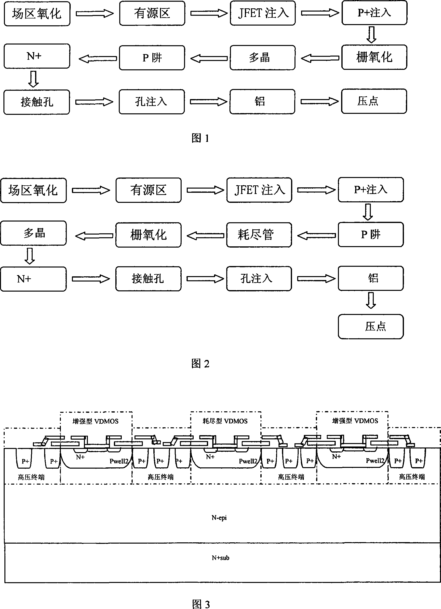
[0039] The N(100) arsenic-doped substrate VDMOS material sheet used has a resistivity of less than 0.005Ω·CM, an epitaxial thickness of 55 μm, and an epitaxial resistivity of 24Ω·CM. On the chip area of ​​2000*2500μm, the strip primitive cell design is adopted, the polycrystalline gate width is 11μm, and the layout method of the enhanced tube surrounds the depletion area, and the corresponding experimental layout design is carried out. According to the adjusted process flow of VDMOS with depletion, the specific implementation method of successfully making enhancement mode and depletion mode VDMOS on the same IC at the same time is as follows:

[0040] 1.) Field region oxidation, the thickness of the oxide layer is 9900-11000 Ȧ.

[0041] 2.) Active area photolithography, etching. Remove the oxide layer in the active area.

[0042] 3.) JFET implantation: implantation energy 100kev; implantation dose 1.2E12; impurity type is phosphorus. The purpose of this injection is mainly ...


PUM


Abstract

The utility model relates to a monolithic fabrication technology for the enhanced and depletion VDMOS, belonging to a technology applying for fabricating a enhanced and a depletion VDMOS with a high voltage (650V) common drain in one IC, which is characterized in that the material of the VDMOS adopting a N(100) substrate doped arsenic, which has a resistivity below 0.005 Omega-CM, the thickness of the epitaxy is 55Mum, the resistivity of the epitaxy is 24 Omega-CM. The withstand voltage can be stable on 650V, and up to 700V. To add a depletion VDMOS on the surface of the enhanced VDMOS, the depletion area needs a individual switching voltage adjustment, which is adding once more VT impurity, while adjusting the pre-and post process. The utility model has the advantages of fewer photoetching, low cost and simple fabricating control.

Description

technical field [0001] The invention relates to a process method for simultaneously manufacturing high-voltage (650V) common-drain enhanced VDMOS and depletion-type VDMOS on the same IC, and belongs to the technical field of semiconductor manufacturing. Background technique [0002] With the continuous development of semiconductor technology, the market application of switching power supply circuits continues to expand. People's awareness of resource protection continues to increase. The requirements for integration and power loss of switching power supply circuits are becoming more and more stringent. In order to adapt to the design of low power consumption, it is necessary to design a depletion-type VDMOS that can be turned off in the enhanced-type VDMOS (vertical double-diffused metal-oxide-semiconductor) part of the power supply output. When the circuit is powered on, the operating voltage of the circuit is not established, the enhanced VDMOS is in the off state, and t...

Claims


Application Information

Patent Timeline
Patent Type & Authority Applications(China)
IPC IPC(8): H01L21/8236
Inventor 朱伟民易法友聂卫东陈东勤
Owner WUXI CRYSTAL SOURCE MICROELECTRONICS CO LTD
Why Eureka
Try Eureka