

Semiconductor memory device
A technology for memory devices and semiconductors, which is applied in semiconductor devices, static memories, electric solid state devices, etc., and can solve the problems of large differences in transistor characteristics and small size.
- Summary
- Abstract
- Description
- Claims
- Application Information
AI Technical Summary
Problems solved by technology
Method used
Image

Examples
Embodiment 1
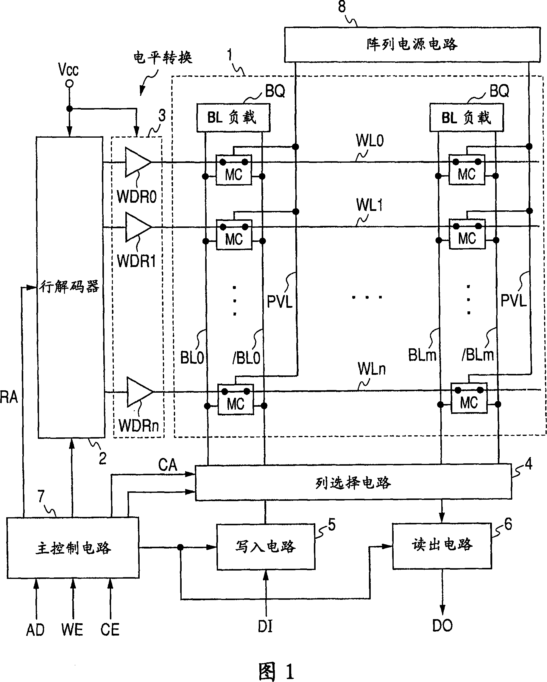
[0038] FIG. 1 is a view roughly illustrating the entire configuration of a semiconductor memory device according to Embodiment 1 of the present invention.
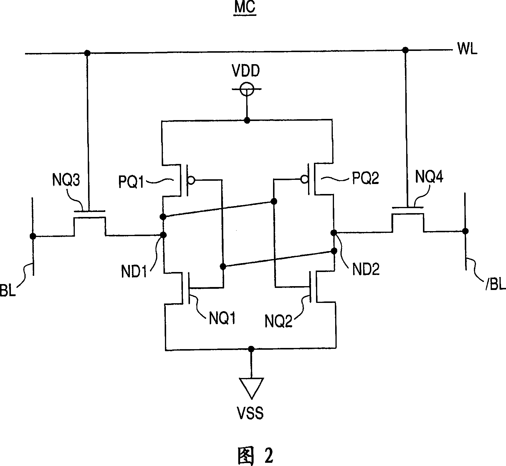
[0039] Referring to FIG. 1, a semiconductor memory device according to Embodiment 1 of the present invention includes a memory array 1 in which memory cells MC are stacked and arranged in a matrix. Memory cells MC are arranged in (n+1) rows (m+1) columns in memory array 1 . Corresponding to each row of memory cells MC, the word lines WL0-WLn are positioned, and the memory cells MC are respectively connected to the word lines of the corresponding row. Corresponding to each column of memory cells MC, a bit line pair BL0, / BL0-BLm, / BLm is located. The memory cell MC is a static type memory cell, as will be described in detail later, and transfers complementary data to a complementary bit line pair BLi, / BLi (i=0~m).
[0040] Corresponding to each pair of bit lines BL0, / BL0-BLm, / BLm, a bit line load (BL load) BQ is formed...
Embodiment 2
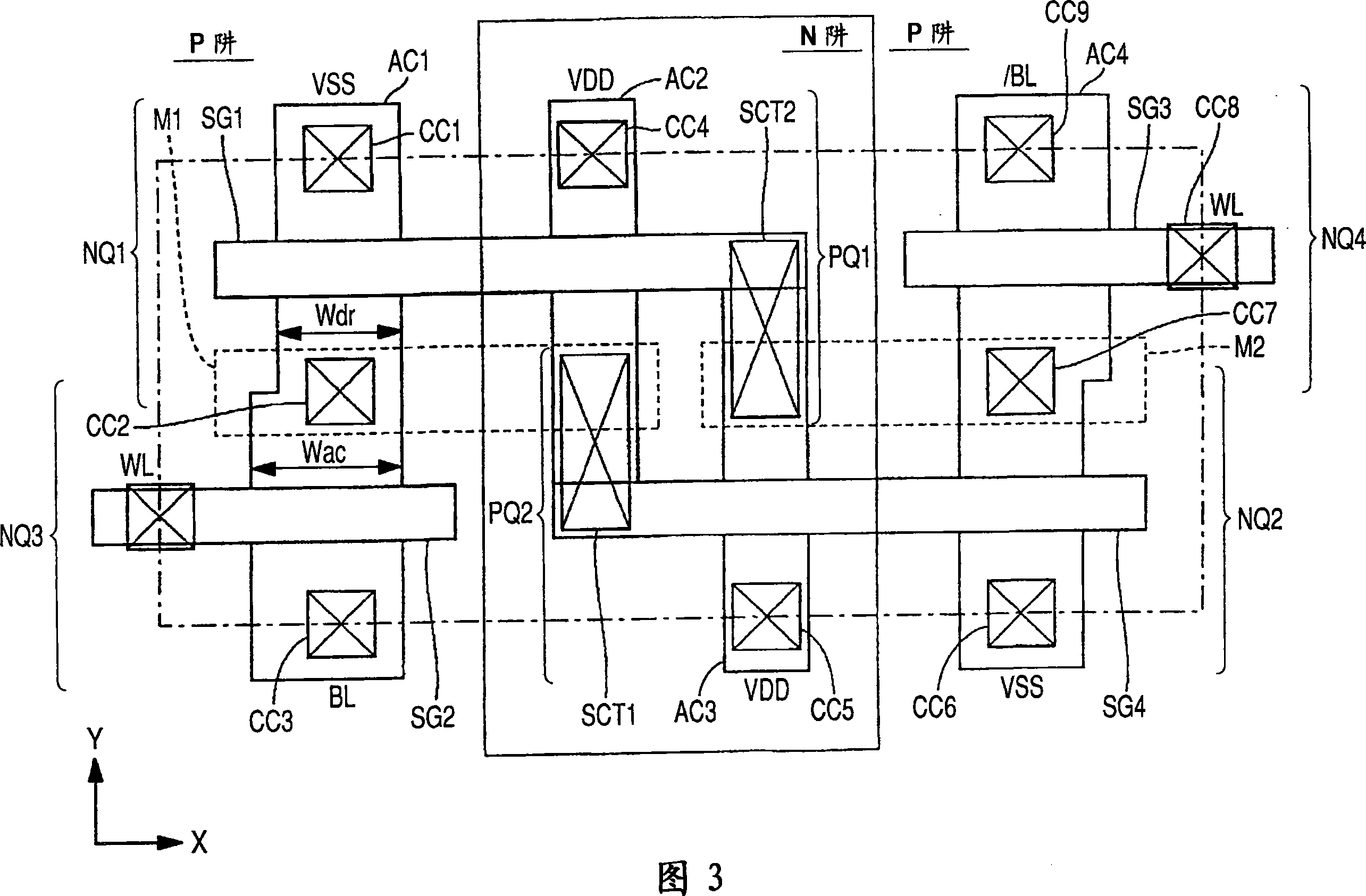
[0088] In the above-described Embodiment 1, a method of suppressing an increase in variation in transistor characteristics was described by making the channel area LW of the access transistor larger than that of the drive transistor designed with the minimum design size. In Embodiment 2 of the present invention, a method for improving the difference in transistor characteristics accompanying gate interdiffusion is described.
[0089] FIG. 8 is a view for explaining gate interdiffusion. Generally, N-type and P-type impurities are each implanted into an NMOS region forming an N-channel MOS transistor and a PMOS region forming a P-channel MOS transistor. However, since the gate of the drive transistor and the gate of the load transistor are a structure in which the gates are shared by a common polysilicon gate as shown in FIG. 8, a PN boundary portion exists within the polysilicon gate electrode.
[0090] 9 is a cross-sectional structure diagram of a driving transistor sharing a...
Embodiment 3
[0140] A method of suppressing variations in characteristics of transistors has been described in the above-described embodiments in conjunction with microfabrication. In general, it is difficult to ensure write and read margins of SRAM memory cells according to microfabrication.
[0141] In Embodiment 3, a method for ensuring write and read margins of SRAM memory cells is described.
[0142] FIG. 15 is a schematic diagram of a word line driver WDV and an auxiliary circuit PD according to Embodiment 3 of the present invention.
[0143] Referring to FIG. 15, the word line driver WDV includes an inverter 10 that receives a word line selection signal WS from the row decoder 2, and a CMOS inverter that inverts the output signal of the inverter 10 and drives the word line WL. P-channel MOS transistors PQ15 and NQ15.
[0144] When the word line WL is selected, the word line selection signal WS is H level, the inverter 10 responds, and its output signal constitutes an L level, and ...
PUM
 Abstract
Description
Claims
Application Information