Method for manufacturing indium column

An indium column and positive adhesive technology, which is applied in the field of semiconductor device and circuit preparation technology, can solve the problems of uncontrollable and difficult to precisely control film thickness, etc., so as to improve welding accuracy, ensure verticality and uniformity, and shorten process time. Effect

Active Publication Date: 2008-02-27
THE 13TH RES INST OF CHINA ELECTRONICS TECH GRP CORP
View PDF0 Cites 6 Cited by
  • Summary
  • Abstract
  • Description
  • Claims
  • Application Information

AI Technical Summary

Problems solved by technology

The equipment is relatively simple, and the source is heated by a resistance wire, and the evaporation rate is fast; but its disadvantage is that it is uncontrollable, and the indium source used for each evaporation needs to be used up once, so the control of the thickness of the indium film depends entirely on the filling amount of the indium source, which is not easy Precise control of film thickness without pretreatment of the indium source surface

Method used


Image

  • Method for manufacturing indium column

Examples


Embodiment Construction

[0028] Below in conjunction with embodiment the present invention is described in further detail:

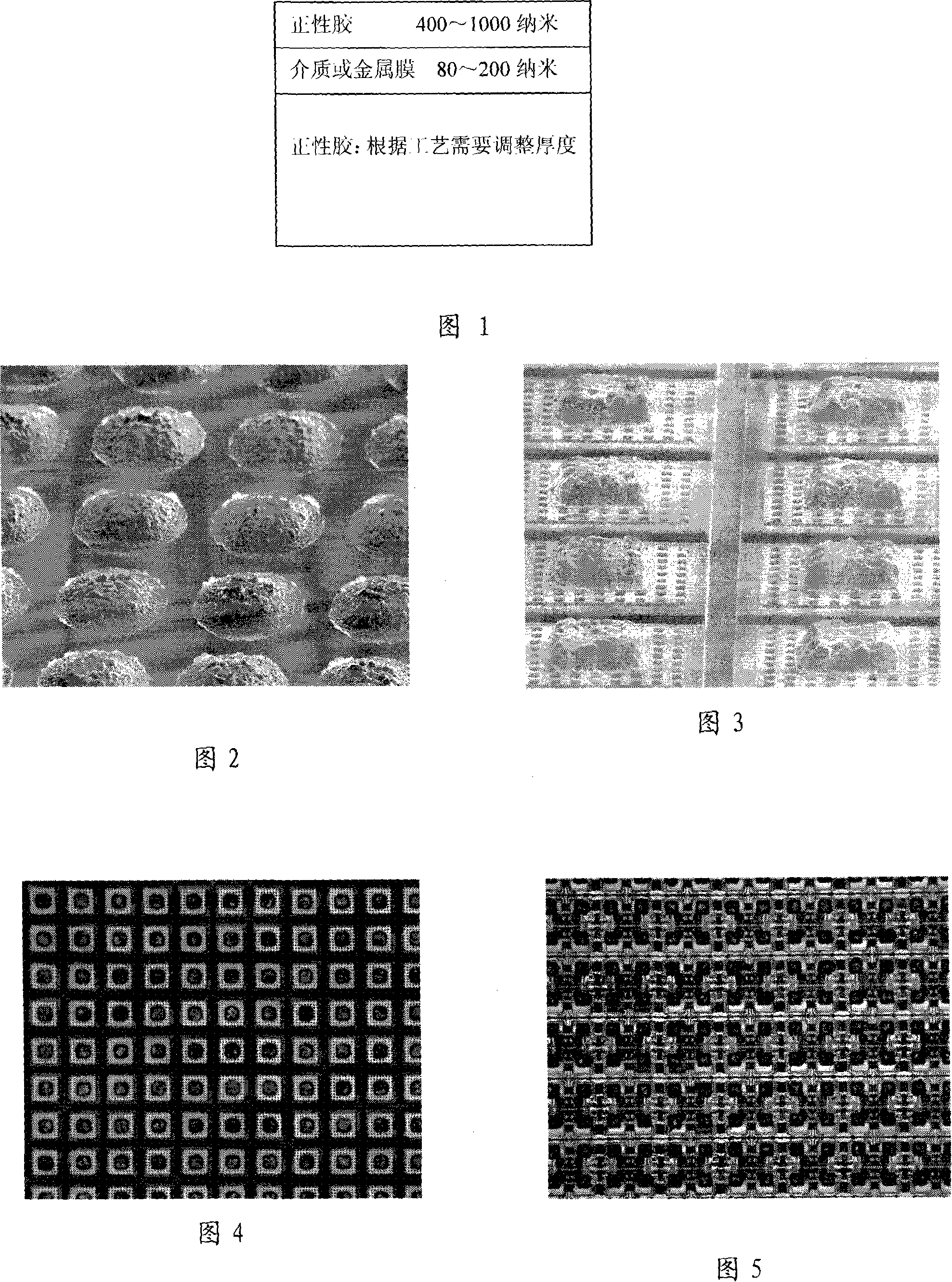
[0029] The indium column we prepared has the following requirements:

[0030] 1) The height of the indium column is 7-8 microns, and the thickness of the photoresist film is not less than 10 microns;

[0031] 2) The photolithographic yield rate is not less than 95%, and the geometric size of the window is ±2 microns from the design value;

[0032] 3) The uniformity of indium film thickness distribution is ±10% of the design value, and the metal surface is smooth and not oxidized;

[0033] 4) The indium film has strong adhesion, and the yield of the indium column after peeling off is not less than 95%.

[0034] The process flow for preparing the above-mentioned indium column is as follows:

[0035] 1. Photolithography process

[0036] 1) Chip treatment: Soak in acetone-isopropanol for several minutes;

[0037] 2) Pre-baking: 100-180°C, 3 minutes;

[0038] 3) Apply the first...


PUM


Abstract

The present invention discloses a method of processing indium cylinder, which is applied to semiconductor device and circuit processing. The method includes the positive-glue photolithography process which has steps of chip processing, pre-baking, glue coating, contraposition, exposure, development, hard baking, and the electron-beam-evaporation-and-micro-ultrasonic-stripping technology which has the steps of chip processing, loading wafer, vacuum pumping, evaporation, taking wafer, stripping. A metal layer or other media films are form between the positive-glue-coated layer to make the coating layer a structure of 'positive glue thick layer - media or metal film - positive glue thin layer', during the glue-coated process; the thin glue on the top are lithographed into patterns, and media or metal films in pattern windows are wet etched, finally, the bottom thick glue is removed by developing and indium film is stripped by electron beam evaporation and micro-ultrasonic stripping. The indium cylinder processed by the present invention has higher precision of its feature than it processed by current technology.

Description

technical field [0001] The invention relates to a semiconductor device and a circuit preparation process, in particular to a detection method for an indium column in a quantum well infrared focal plane detector. Background technique [0002] Quantum well infrared focal plane detector is a new type of infrared detector developed in recent years. It is the development direction of infrared sensing technology at present. It has the advantages of fast response speed, variable wavelength, thermal stability and good uniformity. Occupying an important position in military and civilian use, it has become a frontier topic of high-tech research that is highly valued internationally. [0003] Infrared focal plane array is the core component of modern infrared imaging system. Its manufacturing process is to prepare the detector and signal processing circuit separately first, and then interconnect them together. The interconnection process usually adopts indium column flip-chip intercon...

Claims


Application Information

Patent Timeline
Patent Type & Authority Applications(China)
IPC IPC(8): H01L31/18H01L21/60
CPCY02P70/50
Inventor 冯震杨孟丽
Owner THE 13TH RES INST OF CHINA ELECTRONICS TECH GRP CORP
Why Eureka
Try Eureka