Check patentability & draft patents in minutes with Patsnap Eureka AI!

Flash memory card test device and method

A FLASH memory and daughter card technology, applied in the field of FLASH memory daughter card testing devices, can solve problems such as affecting production costs, being unsuitable for mass production requirements, and low in test efficiency, reducing production costs, improving test pass-through rates, and improving The effect of testing validity

Inactive Publication Date: 2008-03-19
ZTE CORP
View PDF0 Cites 12 Cited by
  • Summary
  • Abstract
  • Description
  • Claims
  • Application Information

AI Technical Summary

Problems solved by technology

[0007] 2) The test efficiency is low, and only one FLASH memory sub-card can be tested at a time, which is not suitable for mass production requirements and affects production costs

Method used


Image

  • Flash memory card test device and method
  • Flash memory card test device and method
  • Flash memory card test device and method

Examples


Embodiment Construction

[0032] The specific implementation of the present invention will be described in further detail below in conjunction with the accompanying drawings.

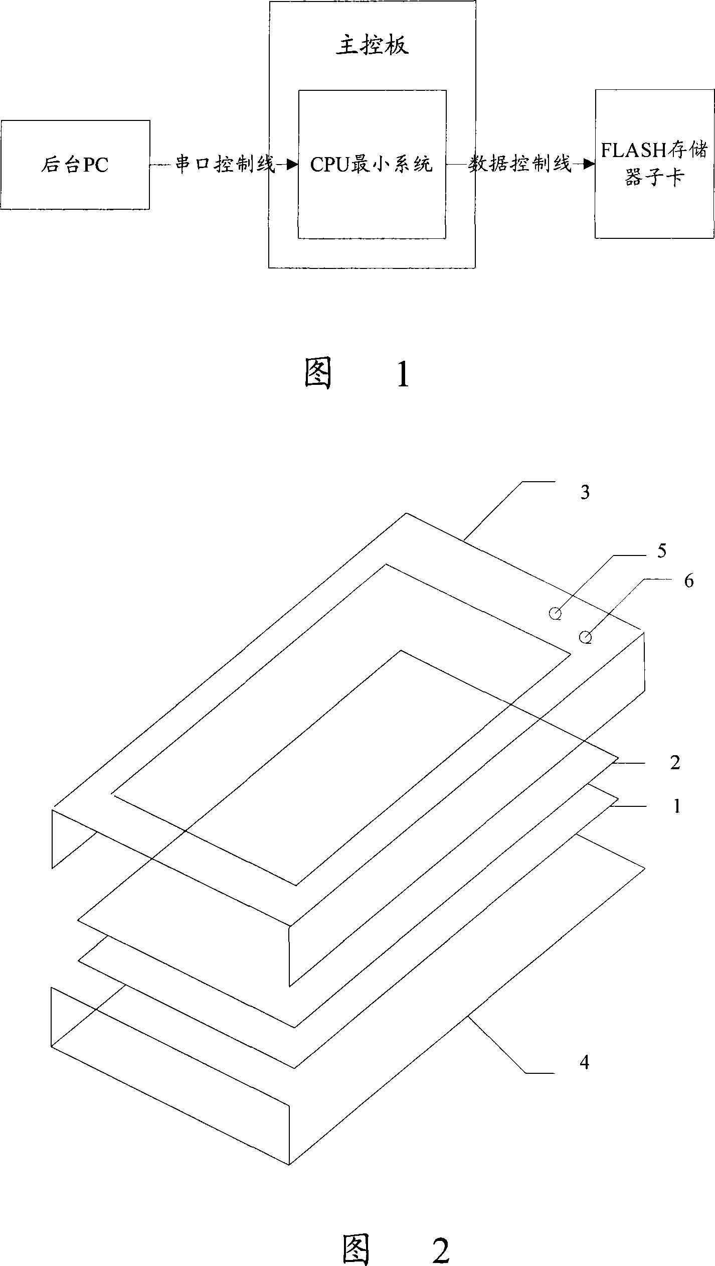
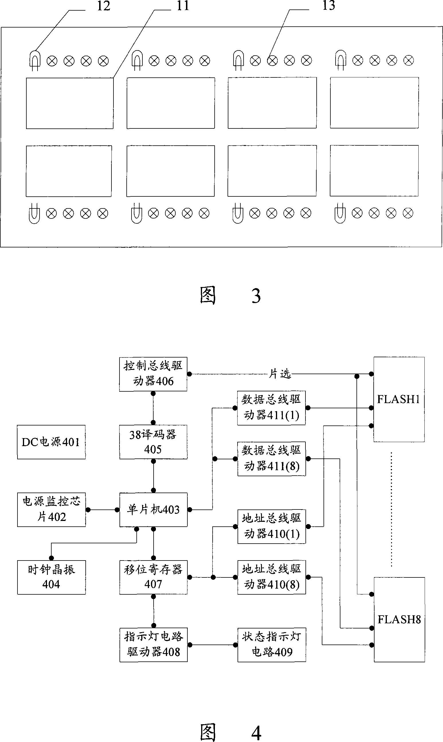
[0033] Figure 2 is a schematic diagram of the appearance structure of the FLASH memory daughter card test device, as shown in Figure 2, the printed circuit board (PCB, Printed Circuit Board) part of the test device is divided into upper and lower parts, and the upper PCB board 2 is a test socket part, that is, the FLASH_TEST part of the top board; the lower PCB board 1 is the microcontroller control part, that is, the FLASH_Control part of the bottom board, and the upper and lower PCB boards are connected by socket plugs, and the FLASH_TEST part of the top board can be used for copying the version of the FLASH memory sub-card. In the present invention, the states of eight FLASH memory sub-cards can be tested at most at the same time, and the version replication of eight FLASH memory sub-cards can be completed. The upper PCB boar...


PUM


Abstract

The invention discloses a flash memory (FLASH) memory sub-card testing device and method. The device comprises: a direct current (DC) power supply, a power supply monitoring chip, a single-chip microcomputer, a clock crystal oscillator, a decoder, a driver, a shift register and a status indicator light circuit; the method comprises: plugging in the FLASH memory sub-card to be tested, turning on the DC power supply, and notifying the single-chip microcomputer to start working after the power monitoring chip completes the power-on reset, and the single-chip microcomputer performs the operation on the FLASH memory sub-card through a decoder and a control bus driver. Chip selection, then test the FLASH memory sub-card by address bus driver and data bus driver, and finally display the test result by the status indicator circuit and the status indicator driver. Utilizing the present invention, up to eight FLASH memory sub-cards can be tested at one time. Improve the production test efficiency and test effectiveness of the FLASH memory daughter card.

Description

technical field [0001] The invention relates to flash memory (FLASH) memory sub-card testing technology, in particular to a FLASH memory sub-card testing device and method. Background technique [0002] FLASH memory has been widely used as a non-volatile storage medium. Usually, several FLASH memory chips are integrated on a small board to make a daughter card, which is connected to the motherboard socket through a standard SODIMM-144 gold finger. , this kind of FLASH memory daughter card will not occupy the space of the motherboard, which has certain advantages in today's small-sized equipment and high-density single board, and this kind of FLASH memory daughter card has good versatility and portability . [0003] Since the FLASH memory sub-card itself cannot be powered on for testing, it must be tested by powering on the motherboard using this sub-card. In this way, due to the welding defects caused by the production process of the FLASH memory sub-card and the quality d...

Claims


Application Information

Patent Timeline
IPC IPC(8): G11C29/56
Inventor 夏伟年
Owner ZTE CORP
Features
  • R&D
  • Intellectual Property
  • Life Sciences
  • Materials
  • Tech Scout
  • Unparalleled Data Quality
  • Higher Quality Content
  • 60% Fewer Hallucinations
Learn More