Fe/MoS2 nano multilayer film and preparation method thereof
A nano-multi-layer and preparation process technology, applied in the coating, superimposed layer plating, solid-state diffusion coating and other directions, can solve the problem of hindering solid lubricity, not having solid lubricating performance, and the unsatisfactory lubricating efficiency of nano-multilayer film. and other problems, to achieve the effect of excellent tribological performance and strong practicability
- Summary
- Abstract
- Description
- Claims
- Application Information
AI Technical Summary
Problems solved by technology
Method used
Image
Examples
Embodiment 1
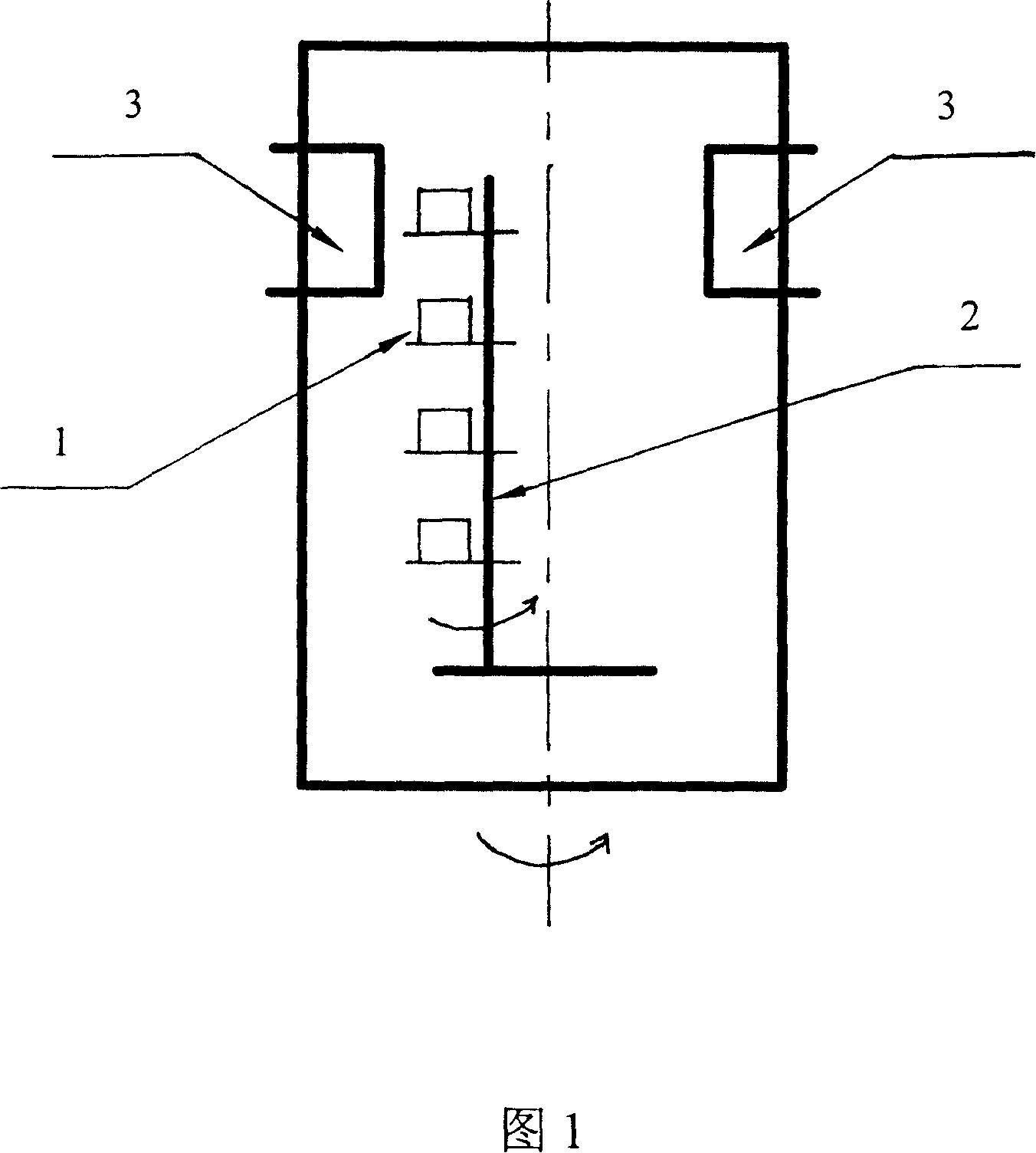
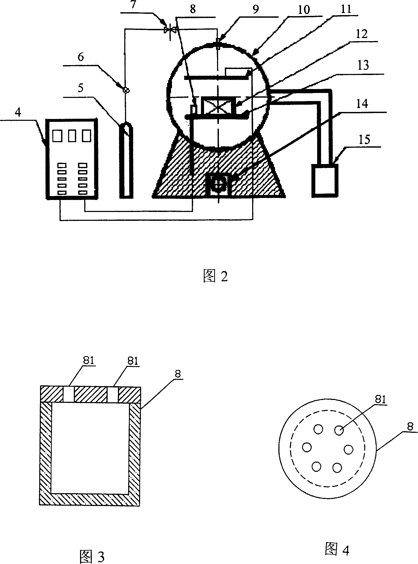
[0043] 1. RF sputtering Fe / Mo nano multilayer film:
[0044] Place the Mo target and the Fe target at the two target source positions respectively;
[0045] The purity of the target material used is: Fe target 90-99.99%; Mo target 90-99.95%;
[0046] The substrate is heated to: 50°C before coating;
[0047] The working gas is: 99.999% high-purity Ar gas;
[0048] Vacuum degree: 2×10 -4 Pa;
[0049] Working air pressure: 2×10 -2 Pa;
[0050] Add negative bias voltage to improve deposition efficiency: 50V;
[0051] Setting voltage: 500V, current 100mA, self-bias 450V, sputtering power 100W;
[0052] When depositing the Mo layer, the residence time of the substrate in front of the Mo target is: 9.37 seconds, and the deposition rate is 16nm / min;
[0053] When depositing the Fe layer, the residence time of the substrate in front of the Fe target is: 10 seconds, and the deposition rate is 15nm / min;
[0054] The thickness of the Fe / Mo nano-multilayer film bilayer is 5nm;
...
Embodiment 2
[0060] 1. RF sputtering Fe / Mo nano multilayer film:
[0061] Place the Mo target and the Fe target at the two target source positions respectively;
[0062] The purity of the target material used is: Fe target 90-99.99%; Mo target 90-99.95%;
[0063] The substrate is heated to: 100°C before coating;
[0064] The working gas is: 99.999% high-purity Ar gas;
[0065] Vacuum degree: 1×10 -2 Pa;
[0066] Working air pressure: 5×10 -1 Pa;
[0067] Add negative bias voltage to improve deposition efficiency: 120V;
[0068] Setting voltage: 800V, current 220mA, self-bias voltage 750V, sputtering power 200W;
[0069] When depositing the Mo layer, the residence time of the substrate in front of the Mo target is: 25 seconds, and the deposition rate is 12nm / min;
[0070] When depositing the Fe layer, the residence time of the substrate in front of the Fe target is: 40 seconds, and the deposition rate is 7.5nm / min;
[0071] The thickness of the Fe / Mo nano-multilayer film bilayer is...
Embodiment 3
[0077] 1. RF sputtering Fe / Mo nano multilayer film:
[0078] Place the Mo target and the Fe target at the two target source positions respectively;
[0079] The purity of the target material used is: Fe target 90-99.99%; Mo target 90-99.95%;
[0080] The substrate is heated to: 150°C before coating;
[0081] The working gas is: 99.999% high-purity Ar gas;
[0082] Vacuum degree: 2×10 -2 Pa;
[0083] Working air pressure: 2×10 0 Pa;
[0084] Add negative bias voltage to improve deposition efficiency: 200V;
[0085] Setting voltage: 1000V, current 400mA, self-bias voltage 950V, sputtering power 300W;
[0086] When depositing the Mo layer, the residence time of the substrate in front of the Mo target is: 100 seconds, and the deposition rate is 6nm / min;
[0087] When depositing the Fe layer, the residence time of the substrate in front of the Fe target is: 100 seconds, and the deposition rate is 6nm / min;
[0088] The finally obtained Fe / Mo nanometer multi-layer bilayer ha...
PUM
| Property | Measurement | Unit |
|---|---|---|
| thickness | aaaaa | aaaaa |
| thickness | aaaaa | aaaaa |
Abstract
Description
Claims
Application Information
 - R&D
- Intellectual Property
- Life Sciences
- Materials
- Tech Scout
- Unparalleled Data Quality
- Higher Quality Content
- 60% Fewer Hallucinations
Browse by: Latest US Patents, China's latest patents, Technical Efficacy Thesaurus, Application Domain, Technology Topic, Popular Technical Reports.
© 2025 PatSnap. All rights reserved.Legal|Privacy policy|Modern Slavery Act Transparency Statement|Sitemap|About US| Contact US: help@patsnap.com


