Electron beam alignment mark manufacture method and its uses

An alignment mark and production method technology, applied to the photoengraving process, circuit, discharge tube and other directions of the pattern surface, can solve the problem that the electron beam exposure machine cannot accurately identify the alignment mark, etc., achieves the ideal of ohmic contact, reduces the Errors and the effect of improving work efficiency

Inactive Publication Date: 2008-03-26
SEMICON MFG INT (SHANGHAI) CORP +1
View PDF0 Cites 10 Cited by
  • Summary
  • Abstract
  • Description
  • Claims
  • Application Information

AI Technical Summary

Problems solved by technology

[0013] In view of this, an object of the present invention is to provide a method for making an electron beam alignment mark, so as to solve the problem that the electron beam exposure machine cannot accurately identify the alignment mark due to changes in the shape of the alignment mark metal after high-temperature annealing
[0014] Another object of the present invention is to provide a method of using electron beam alignment marks to make effective grid lines, so as to solve the problem that the alignment marks cannot be accurately identified by the electron beam exposure machine due to changes in the metal morphology of the alignment marks after high temperature annealing

Method used


Image

  • Electron beam alignment mark manufacture method and its uses
  • Electron beam alignment mark manufacture method and its uses
  • Electron beam alignment mark manufacture method and its uses

Examples


Embodiment

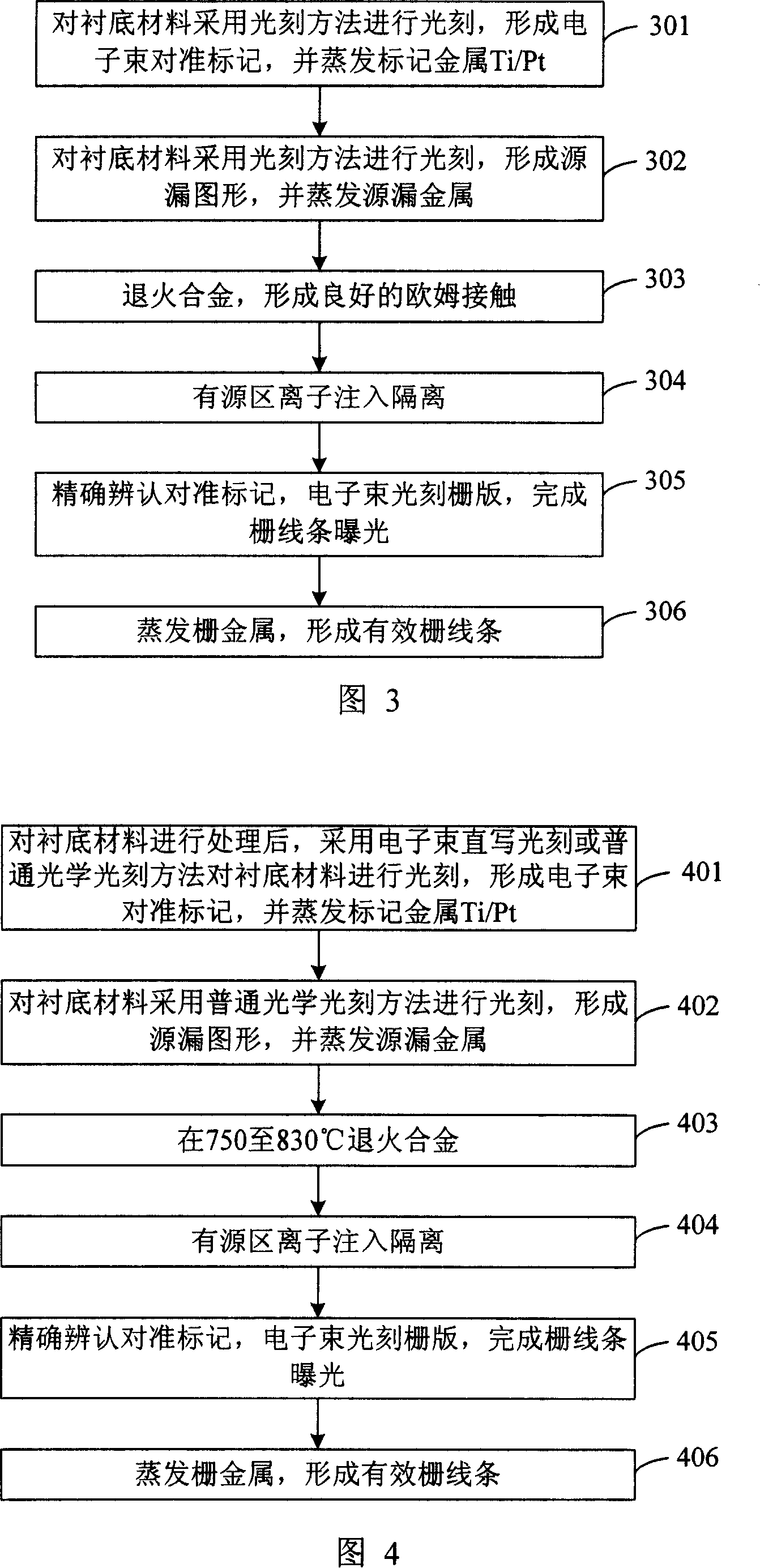
[0057] As shown in FIG. 4, FIG. 4 is a flow chart of a method for making effective grid lines using electron beam alignment marks according to an embodiment of the present invention. The method includes the following steps:

[0058] Step 401: After the substrate material is processed, photolithography is performed on the substrate material by electron beam direct writing lithography or ordinary optical lithography to form an electron beam alignment mark, and evaporate the marked metal Ti / Pt; the mark The metal composition of metal Ti / Pt is: Ti / Pt=60 / 1000 Ȧ.

[0059]Step 402: Perform photolithography on the substrate material by using ordinary optical lithography method to form source and drain patterns, and evaporate source and drain metals;

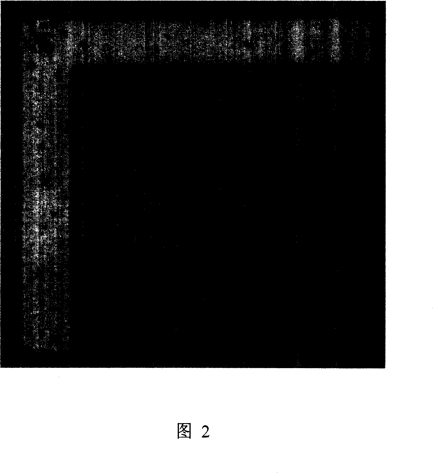
[0060] As shown in FIG. 5 , FIG. 5 is a schematic view showing the morphology of a novel alignment mark metal (Ti / Pt=60 / 1000 Ȧ) structure before annealing manufactured according to an embodiment of the present invention.

[0061] Step 4...


PUM


Abstract

This invention discloses a sort of manufacturing method of the electron beam alignment mark, and it adopts the Ti / Pt metal configuration to be the metal configuration of the alignment mark. It adopts the photo-etching method to process the photo-etching to this underlay material, it forms the electron beam alignment mark in the aluminium-gallium-nitrogen extension layer of the furthest top course of the underlay material. This invention discloses a sort of manufacturing method of the effective bar line by the electron beam alignment mark. A. Adopt the photo-etching method to process the photo-etching to this underlay material, and form the electron beam alignment mark, at last vaporize the marker metal Ti / Pt. B. Adopt the photo-etching method to process the photo-etching to this underlay material, and from the source-drain figure, at last vaporize the source-drain metal. C. Put out a fire to the alloy, and form the good ohm contact. D. Insulate the ion which is in the active area. E. chisel it by the electron beam, achieve the exposal of the bar line. F. Vaporize the bar metal, and form the effective bar line. It availably resolves the problem that the color of the alignment mark metal is changed after the high temperature anneal and it leads that the electron beam exposal device cannot differentiate the alignment mark well and truly by this invention.

Description

technical field [0001] The invention relates to the technical field of manufacturing wide bandgap semiconductor material devices, in particular to a method for manufacturing an electron beam alignment mark and a method for making effective grid lines by using the electron beam alignment mark. Background technique [0002] In the semiconductor field effect transistor structure, the gate length is the most critical factor in determining the frequency of the device. For X-band GaN HEMT devices, in order to obtain a cut-off frequency that is at least 4 times the operating frequency or even higher, the gate length has reached the sub-micron level, and ordinary optical lithography technology is far from meeting our requirements. Require. [0003] Therefore, in the process of fabricating the gate, the direct writing electron beam exposure method with high resolution and overlay precision is adopted, which can produce fine lines of 0.1 to 0.25 microns or even tens of nanometers. ...

Claims


Application Information

Patent Timeline
Patent Type & Authority Applications(China)
IPC IPC(8): G03F7/20G03F9/00H01L21/00H01L21/027H01L21/768H01L21/28H01J37/304
Inventor 刘果果和致经魏珂刘新宇郑英奎
Owner SEMICON MFG INT (SHANGHAI) CORP
Why Eureka
Try Eureka