Method for forming grid side wall layer

A gate sidewall layer and gate technology, which is applied in the direction of electrical components, semiconductor/solid-state device manufacturing, semiconductor devices, etc., can solve the problem of large difference in thermal expansion coefficient of silicon nitride sidewall, insufficient quality of silicon nitride film, Thermal budget advantages are not prominent and other issues, to achieve the effect of improved device performance, good protection, and uniform shape

Active Publication Date: 2008-04-02
SEMICON MFG INT (SHANGHAI) CORP +1
View PDF1 Cites 10 Cited by
  • Summary
  • Abstract
  • Description
  • Claims
  • Application Information

AI Technical Summary

Problems solved by technology

However, the thermal expansion coefficient of the silicon nitride sidewall formed by this method is quite different from that of polysilicon, and it is easy to crack due to temperature rise and fall during the process, and fall off from the polysilicon gate.
In addition, although the deposition temperature of this method is lowered, due to the use of silane (SiH 4 ) or dichlorosilane (SiH 2 Cl 2 ) The deposition rate of the reaction source is low, the required deposition time is long, and the advantages in terms of thermal budget are not outstanding
Moreover, practice has shown that the quality of silicon nitride films grown by this method is not good enough

Method used


Image

  • Method for forming grid side wall layer
  • Method for forming grid side wall layer
  • Method for forming grid side wall layer

Examples


Embodiment Construction

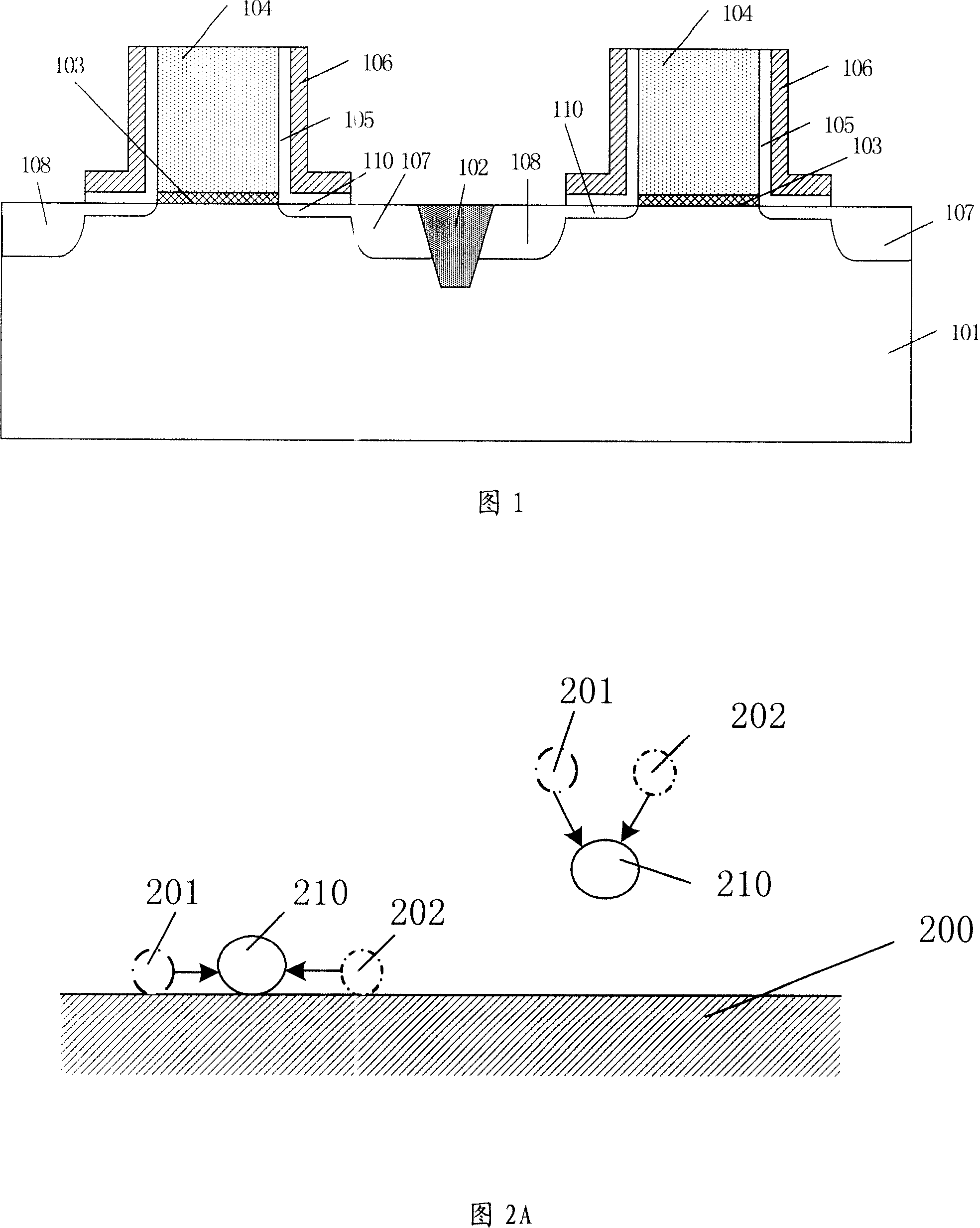
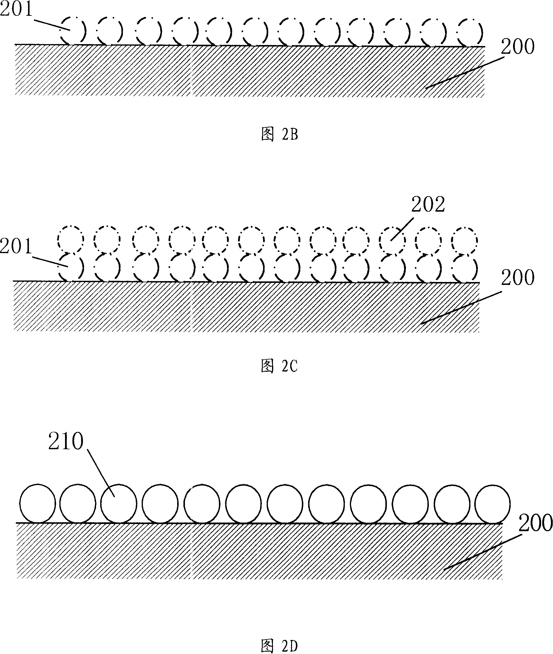
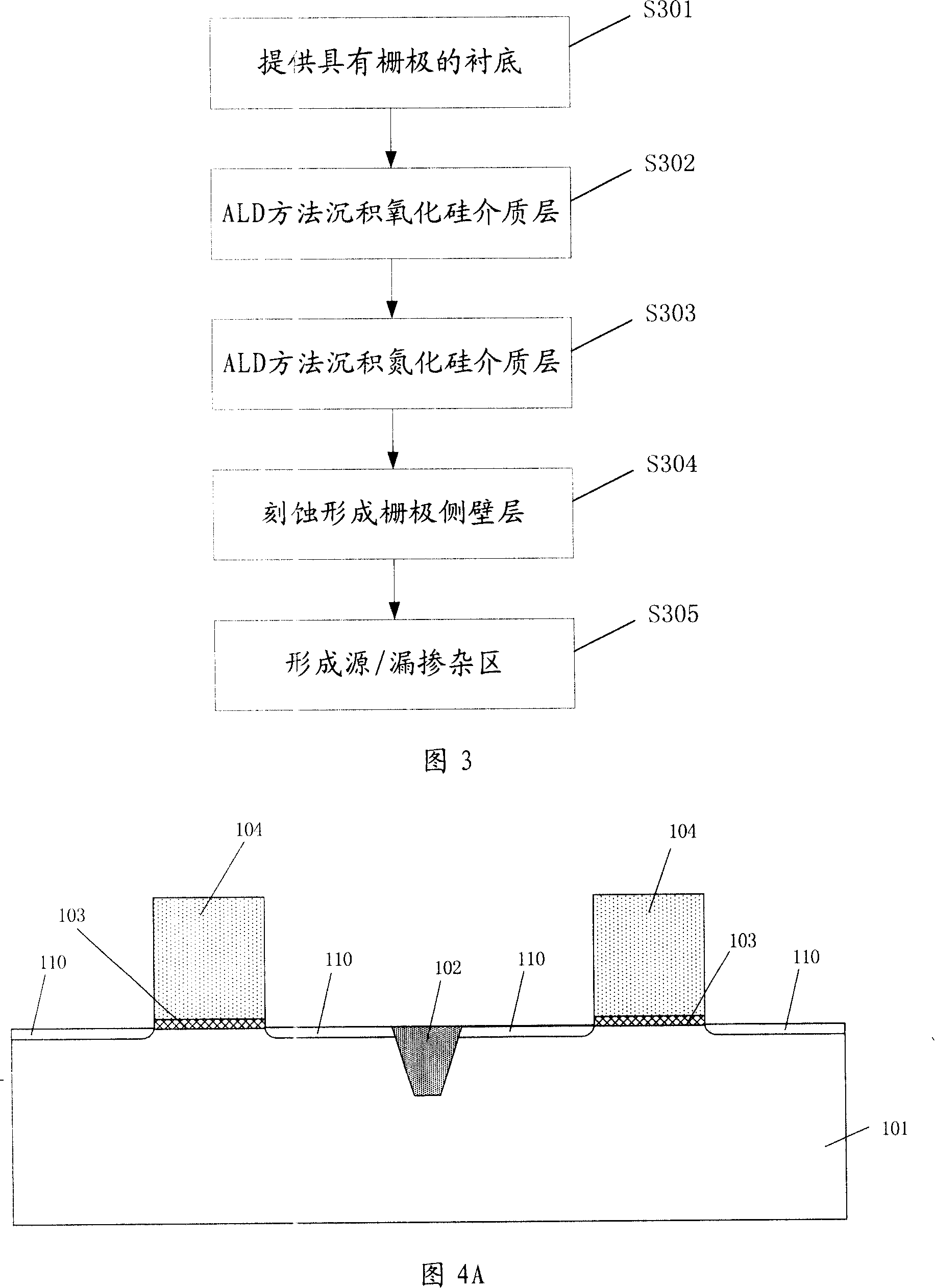
[0049] In order to make the above objects, features and advantages of the present invention more comprehensible, specific implementations of the present invention will be described in detail below in conjunction with the accompanying drawings.

[0050] The processing method of the present invention can be widely applied in many applications, and can utilize many suitable materials to make, and below is to illustrate by preferred embodiment, certainly the present invention is not limited to this specific embodiment, this field Common replacements known to those skilled in the art undoubtedly fall within the protection scope of the present invention.

[0051] Secondly, the present invention is described in detail using schematic diagrams. When describing the embodiments of the present invention in detail, for the convenience of explanation, the cross-sectional view showing the device structure will not be partially enlarged according to the general scale, which should not be used...


PUM

PropertyMeasurementUnit
refractive indexaaaaaaaaaa

Abstract

The invention discloses a method of forming a grid wall layer, including the following steps that: a substrate with at least a grid is provided; the method of atomic layer deposit is utilized to form a complex medium layer in the substrate; a side wall layer is formed in the grid by etching the complex dielectric layer. The invention is not only favorable to improve the performance of the parts with lower heat budgeting, but also improves the uniformity of the performance of the parts with better uniformity of the formed grid side wall layer.

Description

technical field [0001] The invention relates to the technical field of semiconductor manufacturing, in particular to a method for forming a gate sidewall layer. Background technique [0002] The gate sidewall spacer is generally composed of silicon oxide / silicon nitride (ON) dielectric film or silicon oxide / silicon nitride / silicon oxide (ONO) dielectric film combination. [0003] FIG. 1 is a schematic cross-sectional view of a device with an ON structure gate sidewall layer. As shown in FIG. 1, an isolation trench 102 is formed by etching and filling between each device of the substrate, and a gate silicon oxide layer 103 (Gate Oxide) is deposited on the silicon substrate 101; by depositing and etching polysilicon, the A gate 104 is formed on the substrate; on the substrate on both sides of the gate, there is a lightly doped region 110 (LDD, lightly doped drain) formed by shallow ion implantation using the gate as a mask; A gate sidewall layer composed of a silicon oxide d...

Claims


Application Information

Patent Timeline
Patent Type & Authority Applications(China)
IPC IPC(8): H01L21/28H01L21/31H01L21/336
Inventor 何有丰
Owner SEMICON MFG INT (SHANGHAI) CORP
Why Eureka
Try Eureka