Wet oxidation preparation method of Cu2O resistor memory
A resistive memory, wet oxidation technology, applied in the field of microelectronics, achieves the effects of low cost, uniform storage medium, and easy process compatibility
- Summary
- Abstract
- Description
- Claims
- Application Information
AI Technical Summary
Problems solved by technology
Method used
Image
Examples
Embodiment 1
[0068] Example 1, integration with dual damascene process.
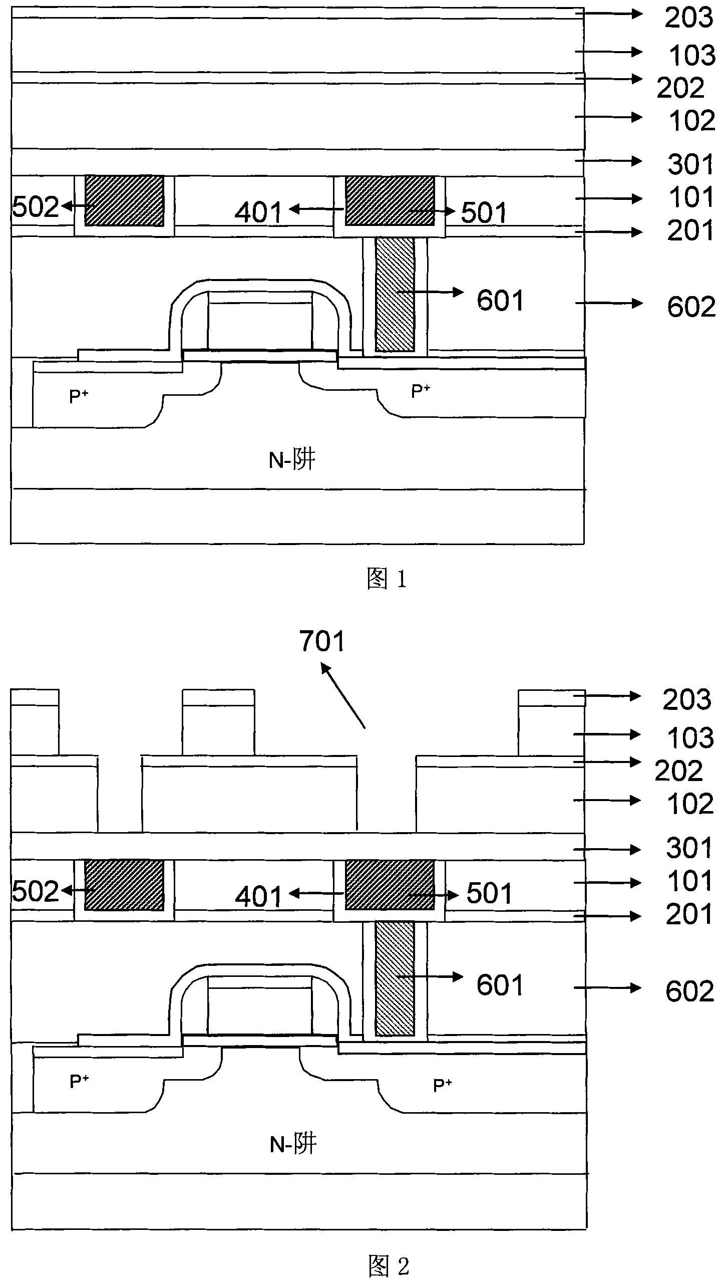
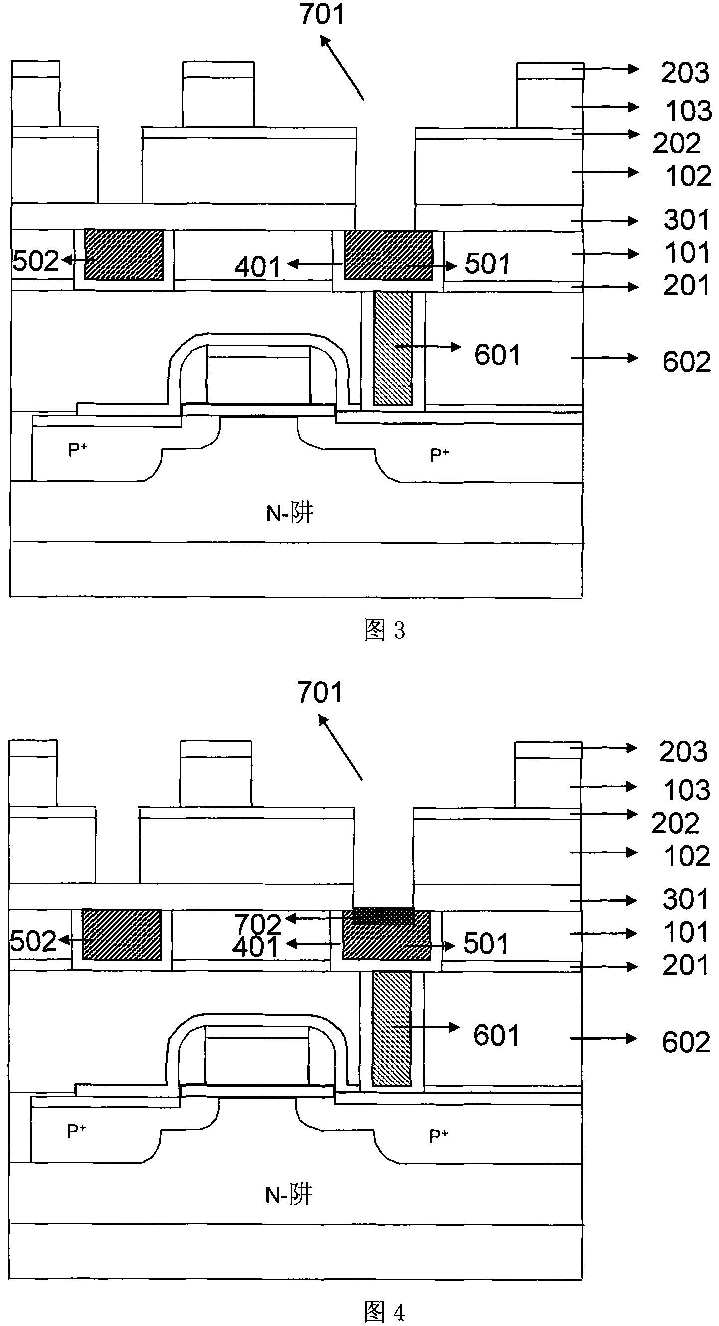
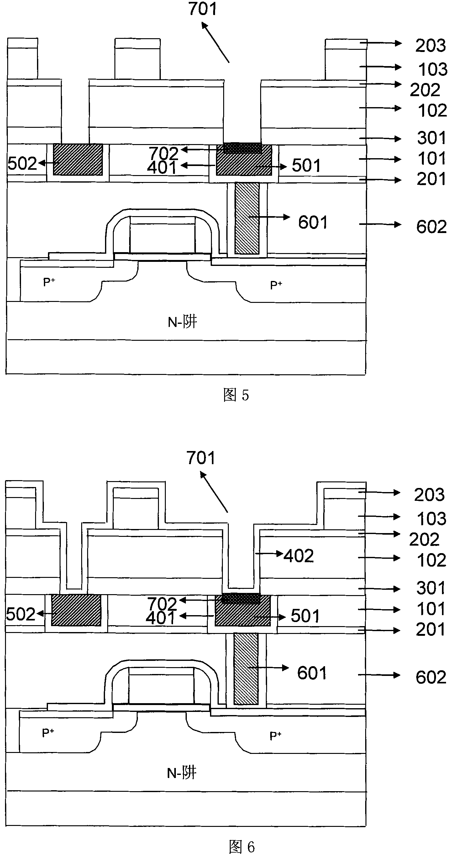
[0069] Figure 1 to Figure 9 is a cross-sectional view according to an embodiment of the present invention. Figure 1 to Figure 9 Shows Cu x Process method of O resistance memory wet oxidation method integrated with double damascene copper interconnection process and formed between the first layer copper lead and the second layer lead, Cu x O is formed on the first layer of copper lines and under the copper plugs. However, the present invention is not limited to this embodiment.
[0070] figure 1 It is a cross-sectional view after the conventional double damascene copper interconnection process, the completion of the first layer of copper wiring, and the deposition of the cap layer, interlayer dielectric (IMD), and etch stop layer. 602 is a PMD layer, which refers to the dielectric layer between the first layer of leads and the MOS device, and it can be a doped silicon oxide layer, such as silicon oxide doped wi...
Embodiment 2
[0091] Example 2, integration with a single damascene process.
[0092] Figure 10 to Figure 20 is a cross-sectional view according to Embodiment 2 of the present invention, Figure 10 to Figure 20 Shows Cu x The process method of O resistance memory wet oxidation method integrated with single damascene process and formed between the first layer copper wiring and the second layer wiring, Cu x O is formed under the second layer of copper lines and above the copper plugs. But the present invention is not limited to this embodiment.
[0093] Figure 10 It shows a cross-sectional view after the conventional single damascene copper interconnection process is completed, the first layer of copper wiring is fabricated, and the cap layer 301 and the interlayer dielectric (IMD) 102 are deposited. 602 is the PMD layer, which refers to the dielectric layer between the first layer of wiring and the MOS device, which can be a dielectric material such as phosphorous-doped silicon oxide ...
Embodiment 3
[0117] Embodiment 3 and above electrode are as the Cu of protective layer structure x O resistance memory manufacturing process integration
[0118] Figure 21 to Figure 35 It is a sectional view according to Embodiment 3 of the present invention. Figure 21 to Figure 35 Shows Cu x Cu prepared by wet oxidation method for O resistance memory with the above electrode as protective layer structure x O-resistance memory manufacturing process is integrated and formed between the first layer of copper wiring and the second layer of wiring, Cu x O is formed on the first layer of copper leads and below the copper plugs. However, the present invention is not limited to this embodiment.
[0119] Figure 21 It shows the cross-sectional view after the conventional double damascene copper interconnection process and the completion of the first layer of copper leads.
[0120] Figure 22It is a cross-sectional view of the capping layer before photolithography, and 301 is a capping la...
PUM
| Property | Measurement | Unit |
|---|---|---|
| thickness | aaaaa | aaaaa |
Abstract
Description
Claims
Application Information


