Field-effect tranisistor realizing memory function and method of producing the same

A field-effect transistor and memory technology, applied in semiconductor/solid-state device manufacturing, semiconductor devices, electrical components, etc., can solve problems such as limiting integration density and affecting reliability, and achieve the effect of great flexibility

Inactive Publication Date: 2008-05-14
PEKING UNIV
View PDF0 Cites 33 Cited by
  • Summary
  • Abstract
  • Description
  • Claims
  • Application Information

AI Technical Summary

Problems solved by technology

However, RRAM needs to be designed into a 1T1C cell structure to realize the memory function, which

Method used


Image

  • Field-effect tranisistor realizing memory function and method of producing the same
  • Field-effect tranisistor realizing memory function and method of producing the same
  • Field-effect tranisistor realizing memory function and method of producing the same

Examples


Embodiment Construction

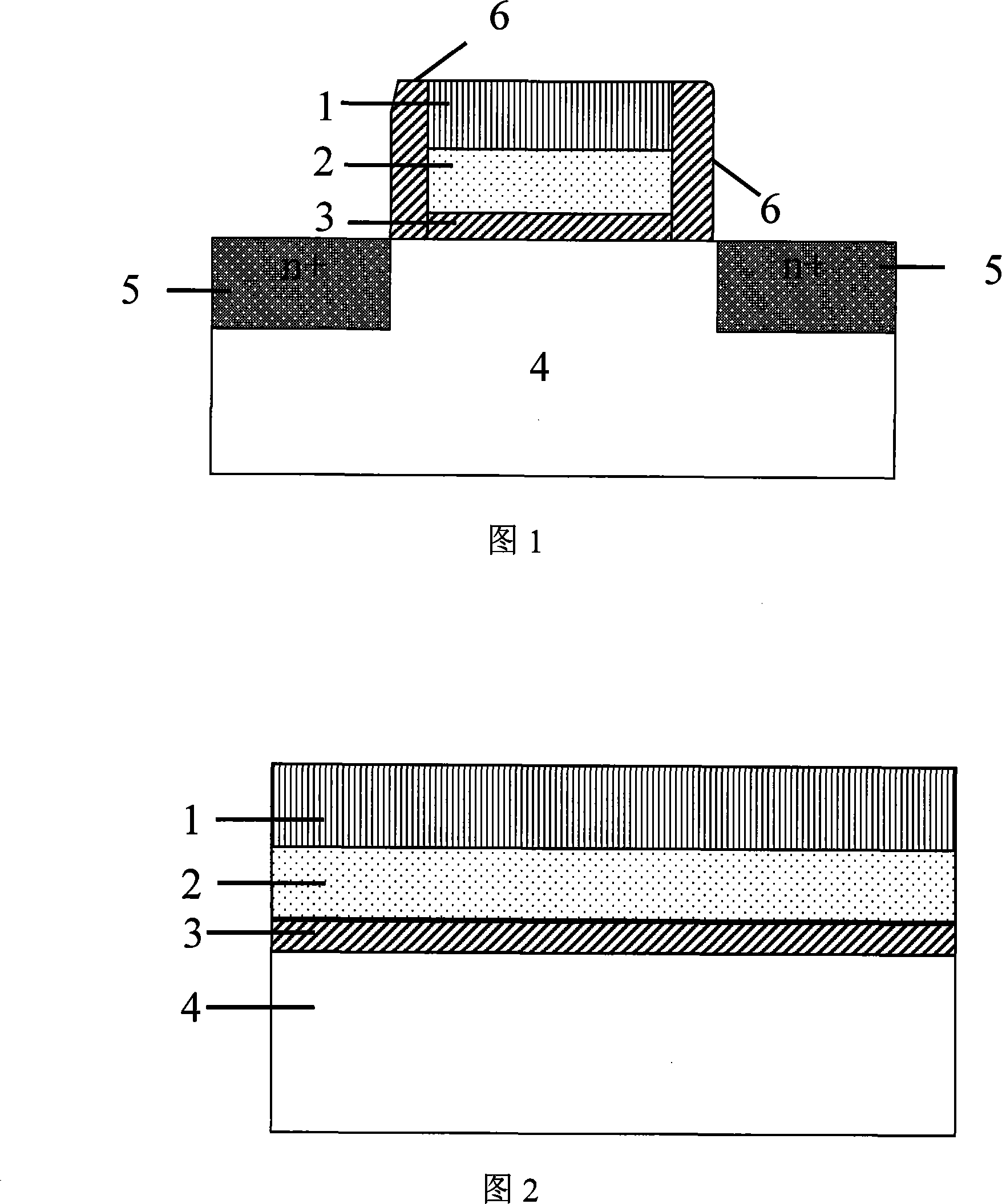
[0036] A cross-sectional view of a field effect transistor (RFET) device proposed by the present invention is shown in FIG. 1 . It includes: a conductive electrode layer 1; a resistive variable dielectric layer 2; a tunnel oxide layer 3; a substrate layer 4; a source region and a drain region 5;

[0037] The specific steps of the resistive field effect transistor preparation process in the present invention are as follows:

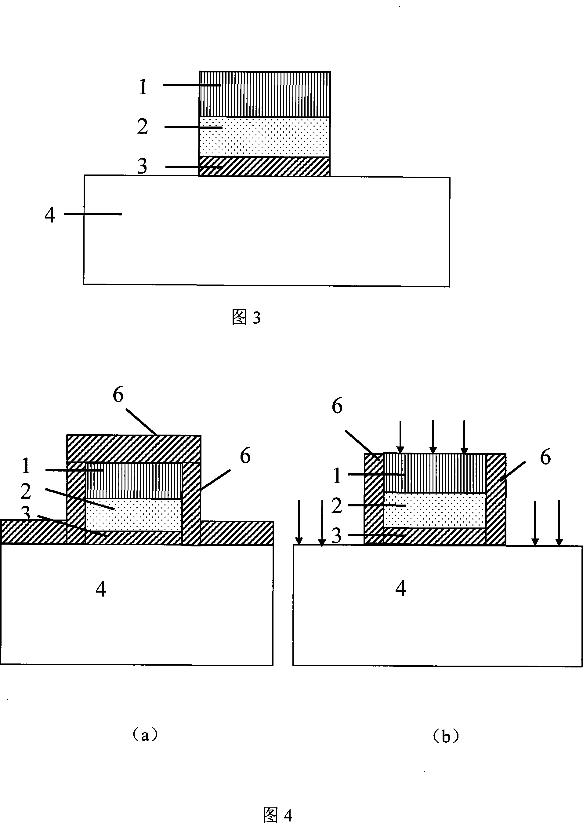
[0038] As shown in FIG. 2 : the thin film deposition process for preparing a resistive field effect transistor. On the cleaned P-type silicon substrate, a thin gate oxide preparation process is used to form a tunneling layer by means of thermal oxidation and rapid thermal annealing (RTP). The thickness of the tunneling layer is 1.5-5nm, and the composition can be silicon dioxide (SiO 2 ), silicon nitride (Si 3 N 4 ) or high-K gate dielectric layer (Al 2 o 3 , HfO 2 Wait). Afterwards, the deposition of the resistive material layer can be performed b...


PUM

PropertyMeasurementUnit
Thicknessaaaaaaaaaa
Thicknessaaaaaaaaaa
Thicknessaaaaaaaaaa

Abstract

The invention provides a field effect transistor that achieves the storage function and the preparation method, which belongs to the filed of semiconductor integrated circuit and manufacturing technology. The transistor comprises a source region, a drain region and a control grid, wherein the control grid utilizes a grid stepped construction which comprises a bottom layer of a tunneling oxidizing layer, an interface layer of a resistance-varying material layer and a top layer of a conductive electrode layer. The field effect transistor obtains an electrically programmable multi-threshold function, the source and drain currents of which are different when a same reading voltage is imposed on the grid, thereby achieving the information storage on two different states or other functions. Utilizing the invention, a plurality of devices and circuits with new functions, high performance and high reliability can be composed, thereby meeting the application of different circuit functions. Meanwhile the invention can adopt the compatibility with the CMOS technology of the conventional PN source or drain junction structure, and can also adopt the compatibility with the CMOS technology of the Schottky source or drain junction structure, with a greater flexibility in technology selection.

Description

technical field [0001] The invention belongs to the technical field of semiconductor integrated circuits and its manufacture, and in particular relates to a field-effect transistor for realizing memory functions and a preparation method thereof. Background technique [0002] The main device in an integrated circuit, especially a very large scale integrated circuit, is a metal oxide semiconductor field effect transistor (MOS transistor for short). Among the MOS-based memory unit circuits, flash memory (Flash) and other mainstream technologies in this field have problems such as high operating voltage, slow speed, and poor endurance. As the size of the device shrinks below 90nm, the characteristics of the flash memory have declined, and it is no longer suitable for further increasing the integration density. The resistive random access memory (Resistive Random Access Memory, referred to as RRAM memory) based on the conductive electrode / resistive material medium has low operat...

Claims


Application Information

Patent Timeline
IPC IPC(8): H01L29/78H01L29/51H01L21/336H01L21/28
Inventor 康晋锋许诺刘晓彦宋云成刘力锋
Owner PEKING UNIV
Why Eureka
Try Eureka