Method for manufacturing AlGaN/GaN-HEMT employing selective regrowth

A manufacturing method and structure technology, which are applied in the field of manufacturing AlGaN/GaN-HEMT using selective regrowth, can solve the problems of AlGaN/GaN-HEMT device characteristic deviation, device reliability deterioration, etching damage and etching end, etc. The effect of maximum drain current and mutual conductance, shortened manufacturing process, and no etching damage

Inactive Publication Date: 2008-05-21
OKI ELECTRIC IND CO LTD
View PDF1 Cites 8 Cited by
  • Summary
  • Abstract
  • Description
  • Claims
  • Application Information

AI Technical Summary

Problems solved by technology

[0020] However, according to the method disclosed in Non-Patent Document 1, n + -In the case of selective regrowth of the GaN layer, there are problems such as impurities deposited on the UID-AlGaN layer or the etched surface of the UID-GaN layer, etch damage, and the shape of the etched end, etc., resulting in the inability to obtain uniform in many cases film quality and film thickness n + -The selective regrowth of the GaN layer cannot obtain a sufficiently low contact resistance value, and the deviation of the value is also large
As a result, the characteristics of the produced AlGaN / GaN-HEMT devices vary, and the reliability of the device deteriorates

Method used


Image

  • Method for manufacturing AlGaN/GaN-HEMT employing selective regrowth
  • Method for manufacturing AlGaN/GaN-HEMT employing selective regrowth
  • Method for manufacturing AlGaN/GaN-HEMT employing selective regrowth

Examples


no. 1 Embodiment approach

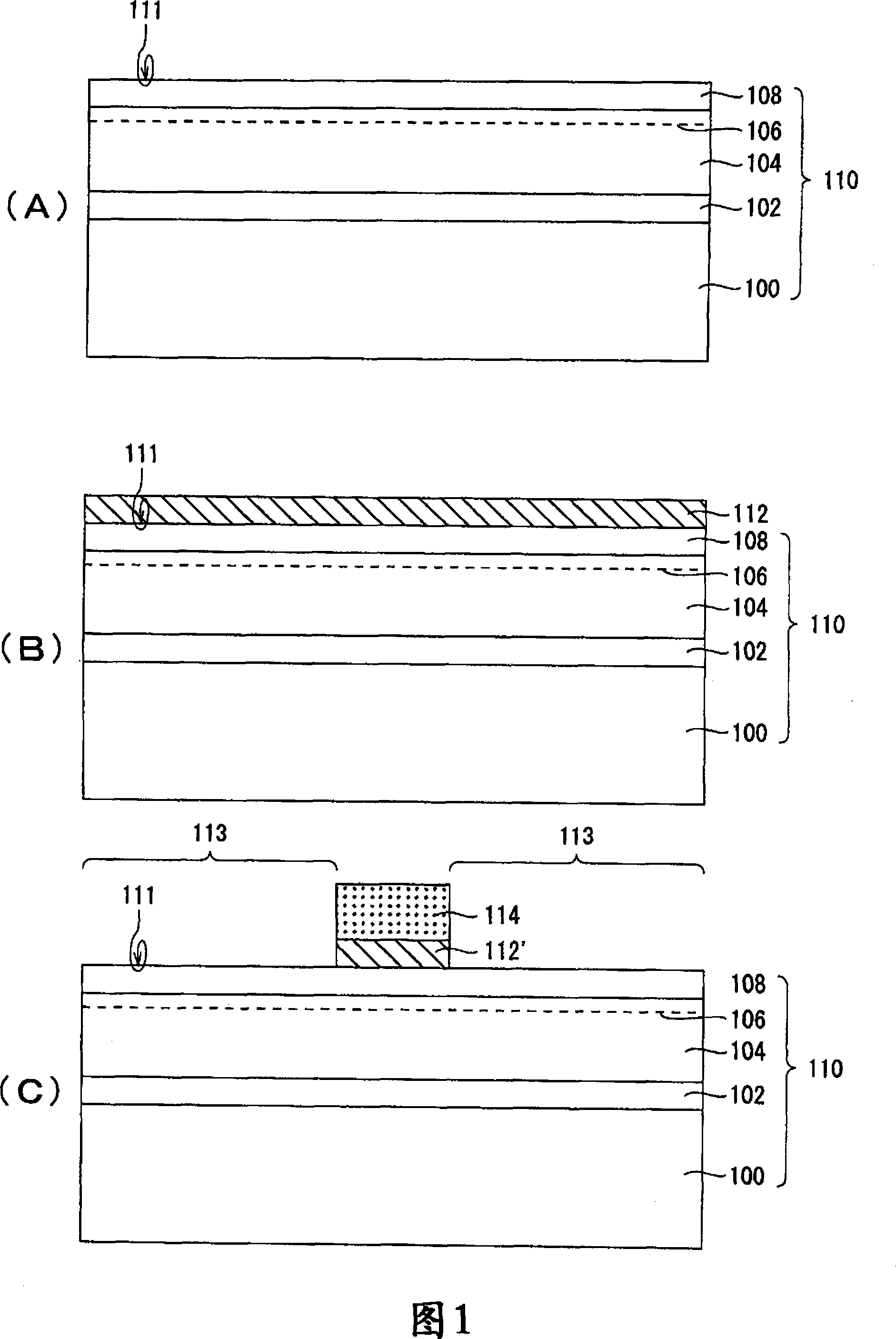
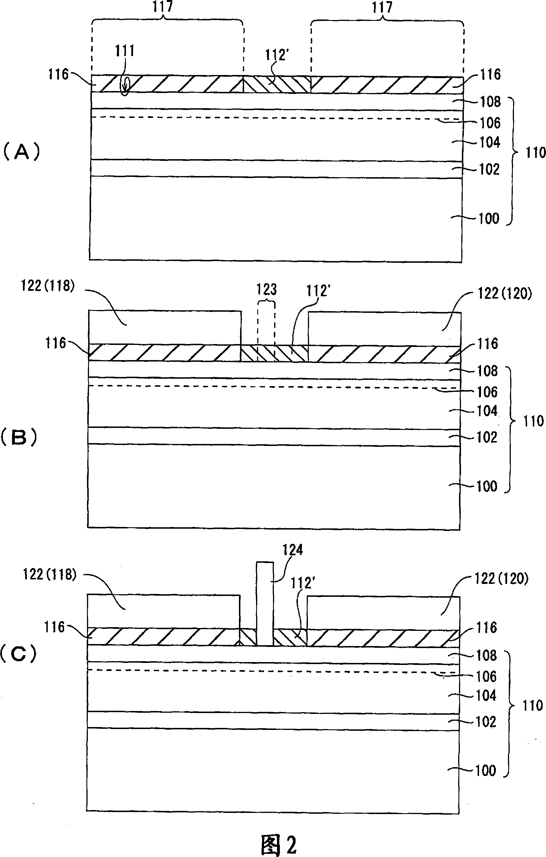
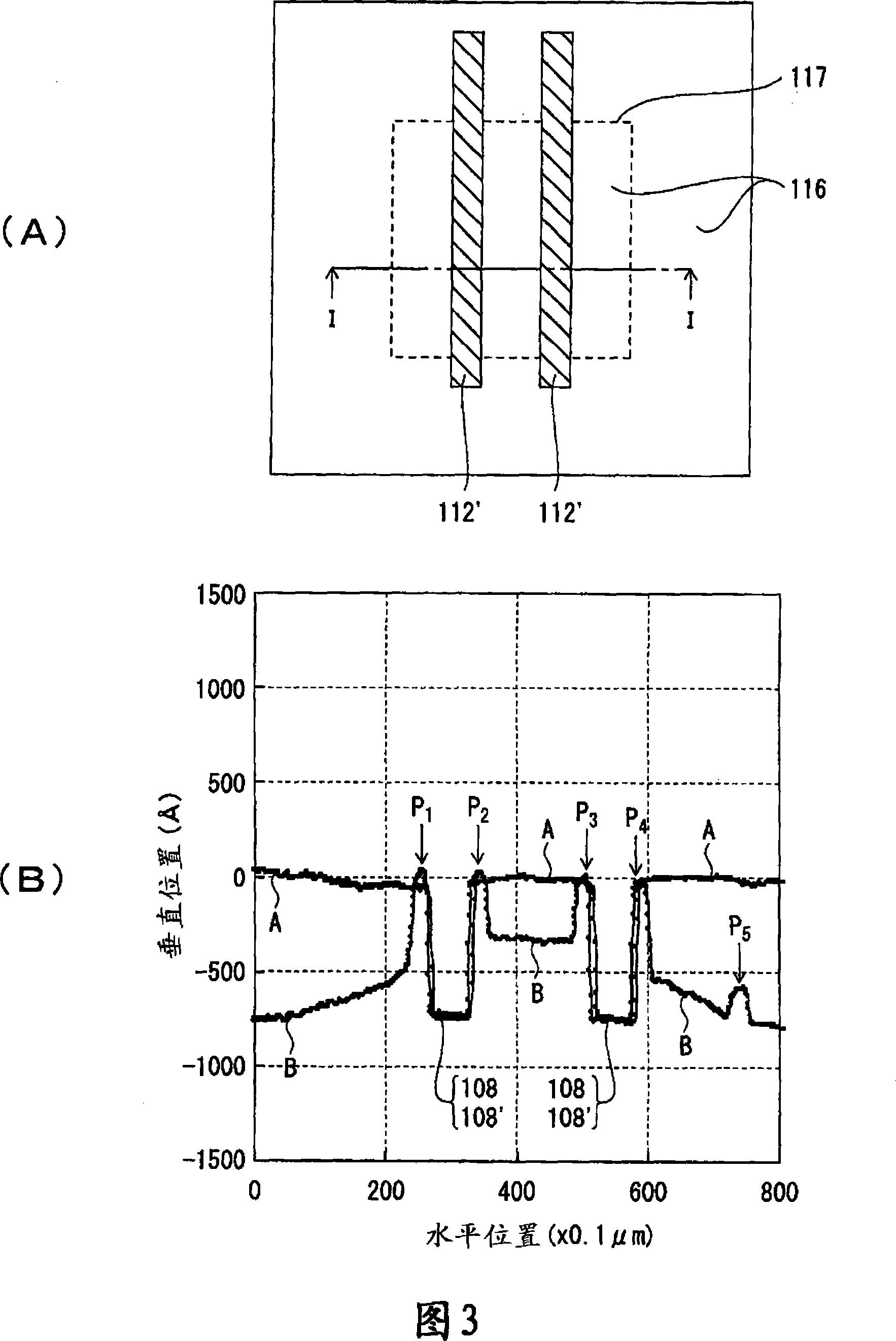
[0049] Fig. 1(A) to Fig. 1(C) and Fig. 2(A) to Fig. 2(C) show the production process flow of AlGaN / GaN-HEMT using selective regrowth for explaining the first embodiment of the present invention summary of . Each figure shows the cross section of the main part of the AlGaN / GaN-HEMT in the main process. Also, in these FIGS. 1 and 2, the same symbols as those in FIGS. 7 and 8 are used for the same elements as those in FIGS. express.

[0050] FIG. 1(A) is a diagram showing a cross-sectional structure of a semiconductor body 110 used in the first embodiment of the present invention.

[0051] First, in the first step, the semiconductor body 110 is prepared. The semiconductor body 110 has a stacked structure in which a HT-AlN buffer layer 102 is stacked on a SI-SiC substrate 100, a UID-GaN layer 104 is stacked on the HT-AlN buffer layer 102, and the UID - formed by laminating a UID-AlGaN layer 108 on the GaN layer 104 . The semiconductor body 110 can be fabricated as follows.

...

no. 2 Embodiment approach

[0080] Next, a MIS-type AlGaN / GaN-HEMT employing selective regrowth according to a second embodiment of the present invention will be described.

[0081] 5 is a view showing a cross section of a main part of an MIS-type AlGaN / GaN-HEMT structure employing selective regrowth for explaining a second embodiment of the present invention. Since the production process and structure are basically the same as those described in the first embodiment of the present invention, they will be briefly described, and in particular, only differences between the second embodiment and the first embodiment will be described. In addition, the same symbols as those in the first embodiment are attached to the symbols of the constituent elements.

[0082] The structures of the Si-SiC substrate 100 and the semiconductor body 110 used are the same as those of the first embodiment.

[0083] Then, on the first main surface 111 of the semiconductor body 110, a 50 nm-thick SiO 2 Layer 112. The SiO 2 The...


PUM


Abstract

The invention relates to a manufacturing method using AlGaN / GaN-HEMT which can selectively revegetate. The method includes preparing a semiconductor main body (110) formed with a laminated structure, which cascades a cushion breaker (102) on a substrate (100), a UID-GaN layer on the cushion breaker, and a UID-AlGaN layer on the UID-GaN layer. The pattern of an insulating film (112) is formed on the first major face (111) of the surface of the semiconductor main body used as the UID-AlGaN layer in order to form a mask of an insulating film (112'). An etching process is not processed on the surface of the semiconductor main body,therefore an nSUP and / SUP-GaN layer selectively revegetates on the surface of the major face (111) of the semiconductor main body apart from the area of the insulating film. An ohm electrode is divided, a preconcerted area (117) is formed and the ohm electrode (122) is formed in the area of the selectively revegetated nSUP and / SUP-GaN layer. Then a preconcerted area (123) is formed and an opening is formed by dividing a gate electrode, and the gate electrode (124) is formed.

Description

technical field [0001] The present invention relates to a method for manufacturing an AlGaN / GaN-HEMT used as a transmitting device and a high withstand voltage switching element of a mobile base station, and in particular to a method for manufacturing an AlGaN / GaN-HEMT using selective regrowth. AlGaN / GaN-HEMTs have ohmic contacts with lower contact resistance values. Background technique [0002] A high electron mobility transistor (High Electron Mobility Transistor: HEMT), which is an electronic device using gallium nitride (Gallium Nitride: GaN), is called AlGaN / GaN-HEMT. The HEMT is formed as follows: using an organic metal Epitaxial crystal growth methods such as Metal Organic Chemical Vapor Deposition (MOCVD) or Molecular Beam Epitaxy (MBE) are sequentially stacked on SiC (Silicon Carbide) substrates, sapphire substrates, or Si substrates. A crystal film of GaN, AlGaN, or the like is grown to form an epitaxial substrate, and the obtained epitaxial substrate is processe...

Claims


Application Information

Patent Timeline
Patent Type & Authority Applications(China)
IPC IPC(8): H01L21/335
CPCH01L29/2003H01L29/7786H01L29/66462H01L29/42316
Inventor 见田充郎户田典彦丸井俊治
Owner OKI ELECTRIC IND CO LTD
Why Eureka
Try Eureka