
Method of identifying crystal defect region in monocrystalline silicon using metal contamination and heat treatment
A technology for crystal defects and single crystal silicon ingots, applied in the directions of post-processing, crystal growth, post-processing details, etc., can solve problems such as inconvenience, inappropriateness, and inability to identify crystal defect areas
- Summary
- Abstract
- Description
- Claims
- Application Information
AI Technical Summary
Problems solved by technology
Method used
Image

Examples
Embodiment 1
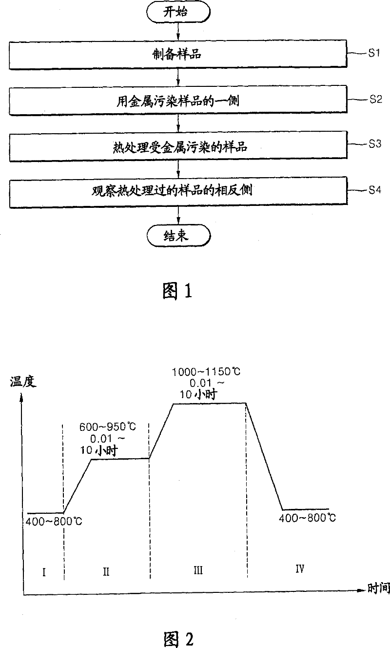
[0063] figure 1 is a flowchart illustrating a method of identifying a crystal defect region according to an exemplary embodiment. figure 2 is to illustrate that according to the exemplary embodiment figure 1 Diagram of the thermal cycle in the identification method.
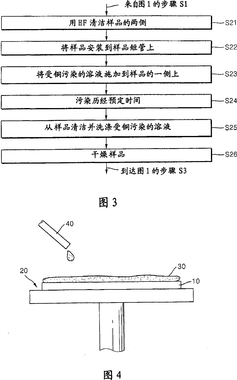
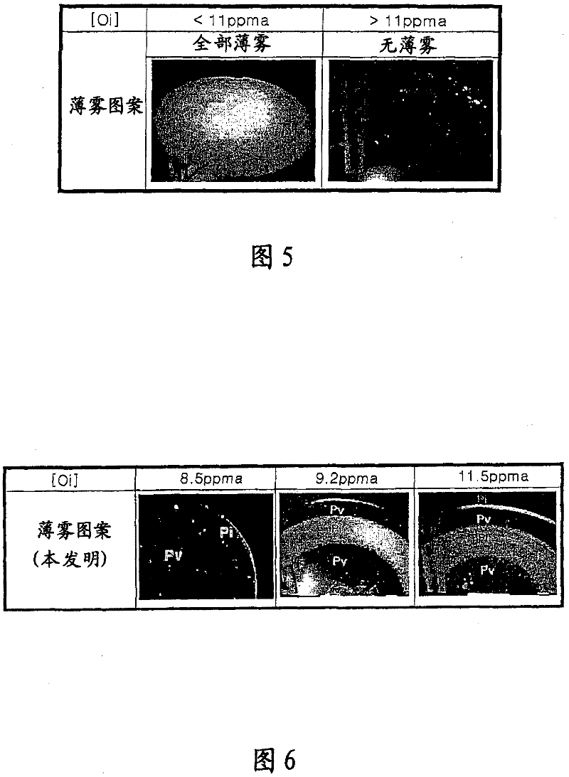
[0064] The present invention prepares samples in the shape of slices of silicon wafers or monocrystalline silicon ingots; contaminates at least one instance of the sample with metal; heat treats the contaminated sample; and visually inspects the contaminated or opposite side of the heat-treated sample under a spotlight to identify crystals defect area. The haze region is interpreted as a Pi region, where interstitial point defects are prevalent but cluster defects are absent; and the non-haze region is interpreted as a Pv region, where vacancy-type points are prevalent defects without cluster defects. For example, a haze pattern can be used to identify crystal defect regions, wherein the haze pattern is gene...
Embodiment 2
[0108] Figure 8 is a flowchart illustrating a method of identifying crystal defect regions according to another exemplary embodiment.
[0109] The present invention can identify all crystal defect regions of single crystal silicon without the need for another analytical method. That is to say, the present invention can simultaneously evaluate all crystal defect regions of single-crystal silicon, such as: Pv regions where vacancy-type defects are common; fine-plate-type precipitates exist; The P-band region where OiSF is generated; the Pi region where interstitial defects are prevalent; the B-band region where oxygen precipitation is generated at high concentrations by seeding heat treatment using interstitial silicon clusters; and the vacancy-rich region where interstitial silicon is prevalent (i -rich region).
[0110] In addition, the present invention can be used for any type of sample with a thickness of about 0.4 to 3 mm. That is, the present invention is applicable t...
PUM
 Abstract
Description
Claims
Application Information