Solid-state imaging device, imaging apparatus and camera

A technology for solid-state imaging devices and imaging devices, applied in semiconductor/solid-state device parts, electric solid-state devices, semiconductor devices, etc., can solve the problem of difficulty in reducing pixel size, disadvantageous high-speed driving, and increasing pixel circuit drive load pixel circuit Problems such as signal readout load

Inactive Publication Date: 2008-05-28
SONY CORP
View PDF3 Cites 15 Cited by
  • Summary
  • Abstract
  • Description
  • Claims
  • Application Information

AI Technical Summary

Problems solved by technology

However, CMOS imaging devices include many driver elements such as photodiodes, transfer transistors, reset transistors, amplification transistors, selection transistors, etc. within one pixel, and thus, it is difficult to reduce the size of the pixels
Also, since the number of pixels is increased, the driving load of the pixel circuit and the readout load of a signal from the pixel circuit are increased, which leads to a situation that is not conducive to high-speed driving

Method used


Image

  • Solid-state imaging device, imaging apparatus and camera
  • Solid-state imaging device, imaging apparatus and camera
  • Solid-state imaging device, imaging apparatus and camera

Examples


no. 3 example

[0112] A third embodiment of the present invention will be described below with reference to the drawings. 8 is a block diagram illustrating one structural example of main units of an imaging device according to a third embodiment of the present invention.

[0113] The imaging device 2001 includes a pixel circuit 2010, a pixel array unit 2011, a horizontal scanning circuit (HSCN) 2012, an amplifier 2121, a vertical scanning circuit (VSCN) 2013, a signal processing circuit 2014, an analog-to-digital converter (A / D) 2015, a timing An adjustment unit 2016 , a timing generator (TG) 2017 , and a lens 2018 .

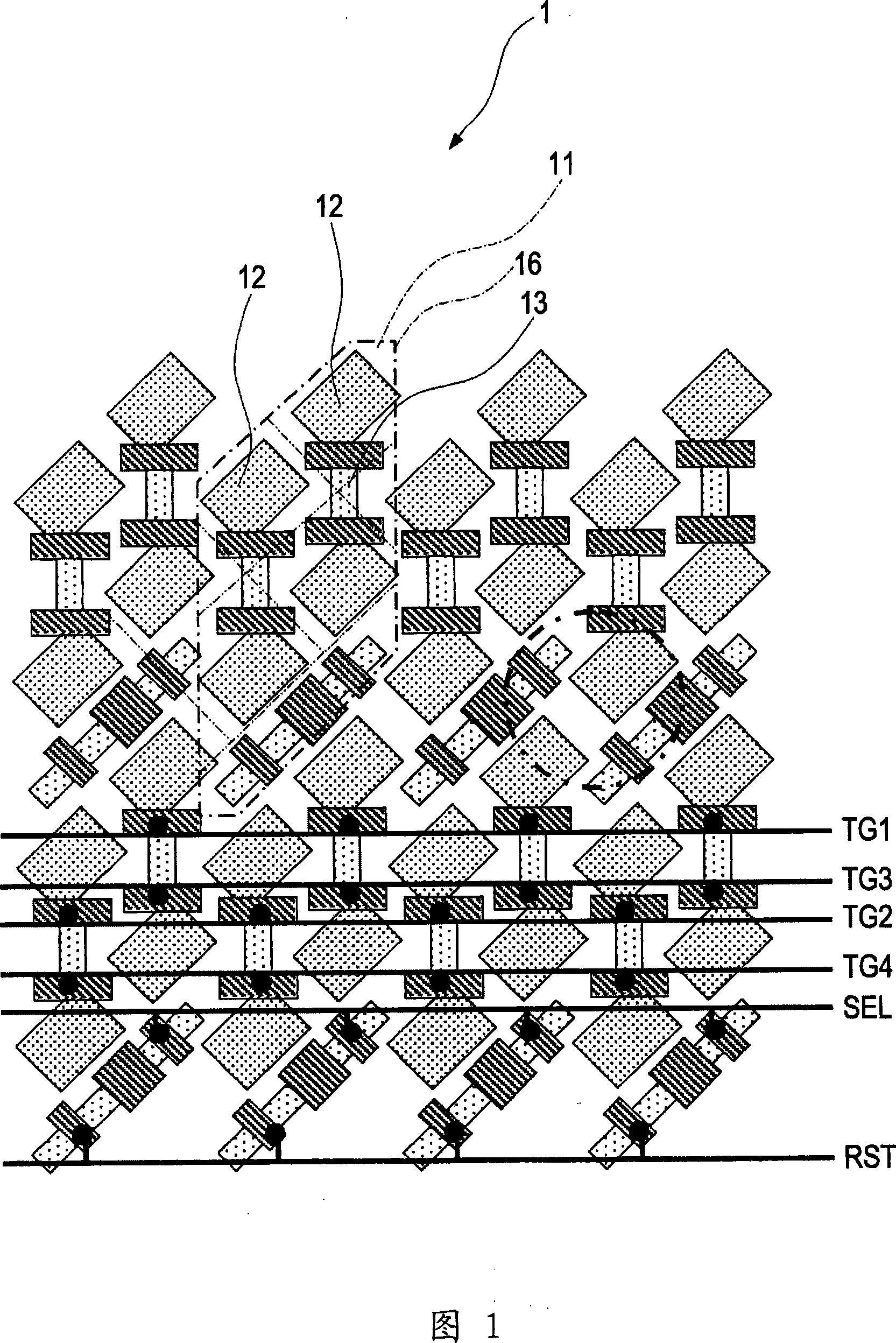
[0114] For the pixel array unit 2011, for example, pixel circuits 2010 are arranged in a matrix shape in a predetermined array pattern.

[0115] Moreover, for the pixel array unit 2011, each row of the vertical scanning circuit 2013 and the pixel array is connected to the reset line RSTL, the transfer selection line TRFL and the selection line SELL, and each row of th...

no. 4 example

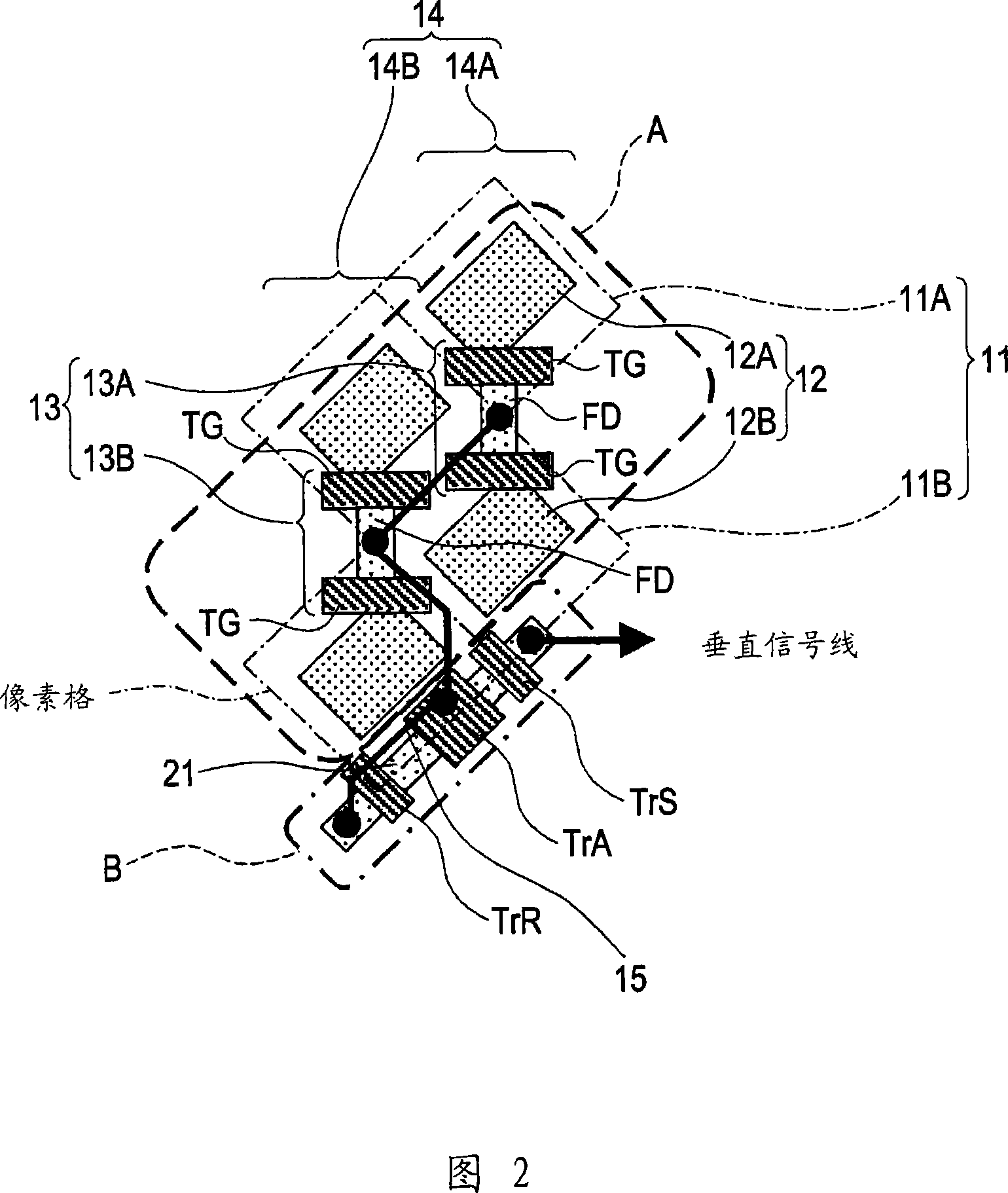
[0172] The following description is about a layout example of a pixel circuit according to a fourth embodiment of the present invention. 13A and 13B are schematic diagrams illustrating one layout example of a pixel circuit according to a fourth embodiment of the present invention.

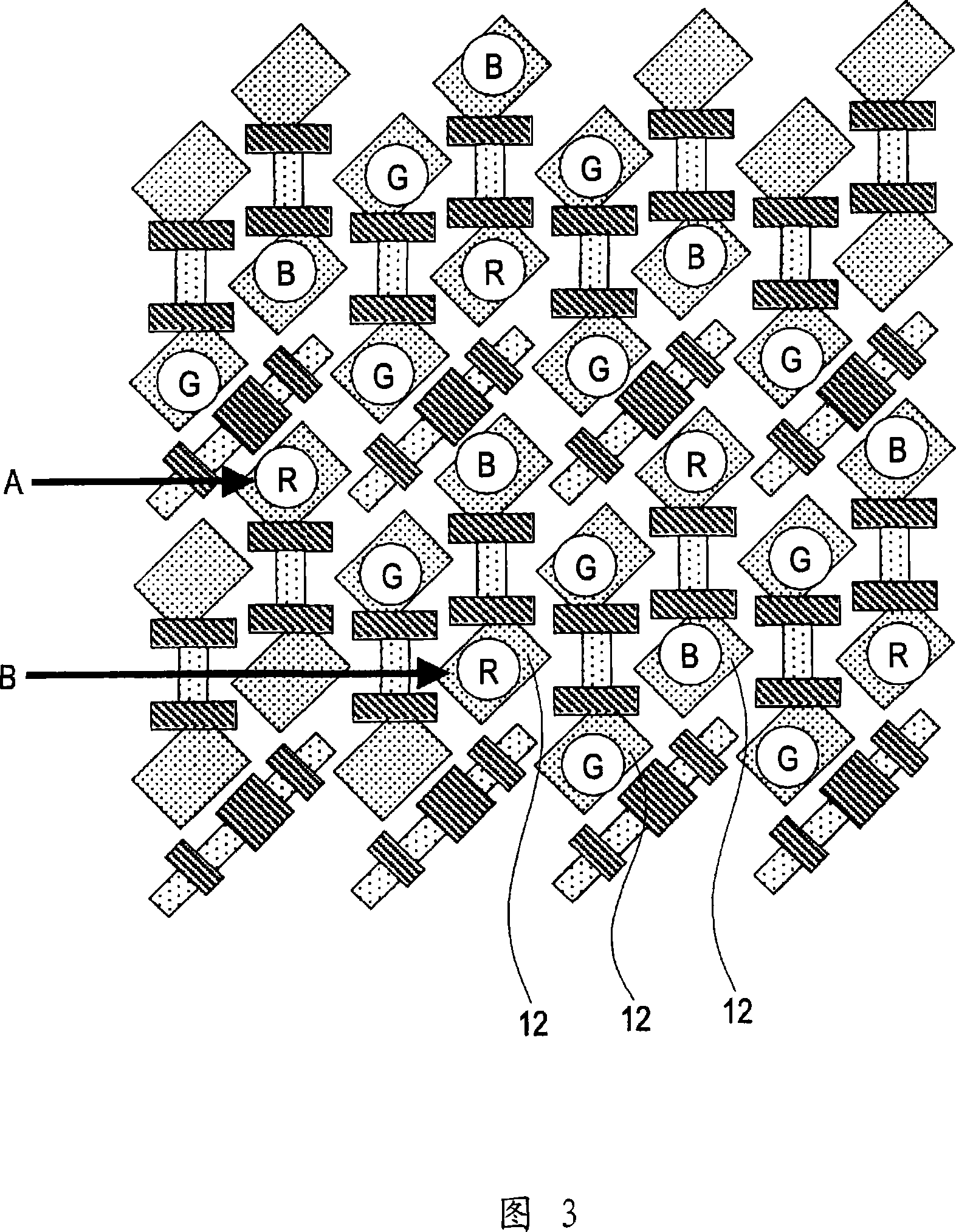
[0173] The pixel group GRP 2002 shown in FIG. 13A is an example in which the two pixel circuits shown in FIG. 9A share the source diffusion layer 2210a of the amplification transistor, and the two pixel circuits 2002a are arranged on the source diffusion layer of the amplification transistor. On the diagonal direction of 2210a. FIG. 13B is an equivalent circuit diagram of the pixel group GRP 2002 shown in FIG. 13A .

[0174] Pixel group GRP 2002 shown in FIG. 13B is an example in which two unit equivalent circuits 2002b shown in FIG. 13B share signal output terminal 2211b and are arranged in a diagonal direction of signal output terminal 2211b.

[0175] FIG. 14 is a schematic diagram in w...

no. 5 example

[0233] Next, a fifth embodiment of the present invention will be described with reference to the drawings. FIG. 16 is a block diagram illustrating one structural example of main units of an imaging apparatus according to a fifth embodiment of the present invention.

[0234] The imaging device 2001a includes a pixel circuit 2010, a pixel array unit 2011, a horizontal scanning circuit (HSCN) 2012a, an amplifier 2121, a vertical scanning circuit (VSCN) 2013, a signal processing circuit 2014, an analog-to-digital converter (A / D) 2015, a timing Adjustment unit 2016a, timing generator TG (2017) and lens 2018.

[0235] The timing adjustment unit 2016a is arranged inside the horizontal scanning circuit 2012a, delays the analog signal input from the pixel array unit 2011 through the amplifier 2121 by a predetermined time according to a predetermined program, and outputs it to the signal processing circuit 2014. The operation of the timing adjustment unit 2016 will be described b...


PUM


Abstract

A solid-state imaging device comprising: a plurality of pixels constituting an oblique grid array inclined to a scanning direction, which includes a photoelectric conversion unit for converting an incident light amount into an electric signal; A charge-to-voltage conversion unit that converts the output signal charge into a voltage, and the photoelectric conversion unit is arranged between two pixels adjacent to each other in a diagonal direction of the plurality of pixels; wherein the charge-to-voltage The conversion unit is shared by the two pixels; wherein a set of transistor groups is arranged in a shared block composed of a pixel pair consisting of two pixels adjacent to each other along a diagonal line, and Pixel pairs adjacent to the pixel pair include wiring connected to the charge-to-voltage conversion unit of each pixel pair.

Description

[0001] Cross References to Related Applications [0002] The subject matter contained in this disclosure is related to Japanese Patent Application JP 2006-279733 filed with Japan Patent Office on October 13, 2006, Japanese Patent Application JP 2006-306278 filed with Japan Patent Office on November 13, 2006, and Japanese Patent Application JP 2006-306278 filed with Japan Patent Office on March 2, 2007. Japanese Patent Application JP2007-052935 filed by the Japan Patent Office, the entire contents of which are hereby incorporated by reference. technical field [0003] The present invention relates to a solid-state imaging device and an imaging device. And, the present invention also relates to an imaging device and a camera including an imaging device such as a CCD (Charge Coupled Device), a CMOS (Complementary Metal Oxide Semiconductor) sensor, or the like. Background technique [0004] Since digital cameras have been widely used in recent years, even low-priced cameras req...

Claims


Application Information

Patent Timeline
Patent Type & Authority Applications(China)
IPC IPC(8): H01L27/146H01L23/522H04N5/335H04N3/15H04N5/369H04N5/374
Inventor 工藤义治
Owner SONY CORP
Why Eureka
Try Eureka