Silicon thin-film photocell electric pole pattern and etching method

A technology of electrode patterns and photovoltaic cells, which is applied in the direction of circuits, electrical components, and climate sustainability, can solve problems such as environmental and equipment pollution, complex processes, and impact on battery electrical performance, and achieve low equipment investment, simplified processes, and improved products. quality effect

Inactive Publication Date: 2008-06-04
李毅
View PDF2 Cites 15 Cited by
  • Summary
  • Abstract
  • Description
  • Claims
  • Application Information

AI Technical Summary

Problems solved by technology

Using this method to etch the aluminum film requires an etching tank to contain the etching solution. The process is complex, requiring multiple processes before and after, and a large amo...

Method used


Image

  • Silicon thin-film photocell electric pole pattern and etching method
  • Silicon thin-film photocell electric pole pattern and etching method
  • Silicon thin-film photocell electric pole pattern and etching method

Examples


example 1

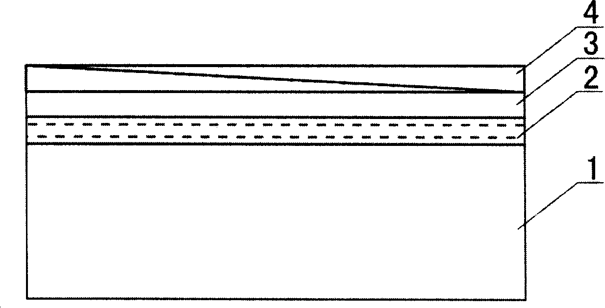
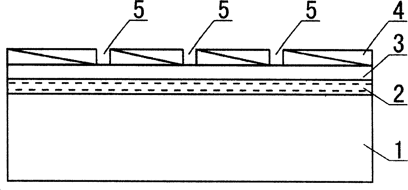
[0048] image 3 It is a schematic diagram of this embodiment, an amorphous silicon solar cell, the shape is a common and commonly used solar cell, and there are several equidistant corrosion isolation lines. according to image 3shape, prepare the wire mesh. Take 50 grams of deionized water, 10 grams of copper sulfate, 20 grams of ferric chloride, and 0.5 grams of ammonium persulfate, add them to the container one by one, stir to dissolve, then add 30 grams of starch, stir to thicken, then add 0.3 grams of defoamer W-090 and 10 grams of absolute ethanol are stirred to make etching ink. Etching ink is screen-printed onto the surface of the aluminum film. Place it horizontally for 3 minutes, so that the aluminum film on the etching line reacts completely with the etching ink, and there is no breakpoint on the etching line. Bake in a 100°C oven for 30 minutes. After cooling, rinse the ink and metal impurities on the aluminum film with clean water. Soak in clean water for 40...

example 2

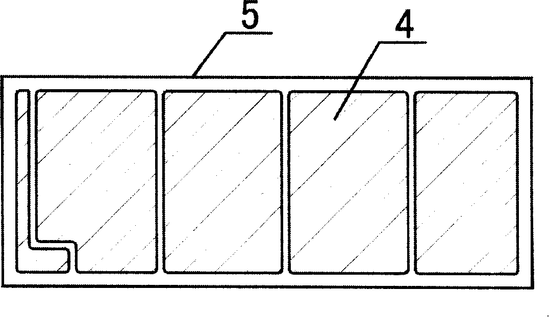
[0050] Figure 4 , which is a circular solar cell, used in products with circular windows, such as clocks and other electronic products. There is a circular window in the middle of the solar cell, and there are corrosion isolation lines beside it. First, prepare Figure 4 Shaped wire mesh. Take 55 grams of water, 8 grams of copper sulfate, and 22 grams of ferric chloride, and add them to the container in turn. After stirring, add 35 grams of starch, stir and thicken, then add 11 grams of absolute ethanol and 0.5 grams of defoamer W- 090, made of etching ink after stirring. Slip-print the etching ink on the surface of the aluminum film and place it horizontally for 5 minutes. After the aluminum film is completely corroded, put it in an oven at 80°C for 40 minutes. After cooling, rinse the aluminum film with clean water for 1 minute, so that the impurities on the corrosion line and the corrosion surface of the aluminum film are completely washed away, and then soak in a clea...


PUM


Abstract

The invention relates to an etching technology for etching a pattern on a photocell with a silicon film, and an etching agent as well as an etching method for manufacturing amorphous silicon solar cells and a pattern on an aluminum dorsal electrode. The purpose of the invention is to provide a cell with a silicon film with a complicated pattern, a method for etching an aluminum film, and an etching agent. Printing ink etched by a silk-screen is unlikely to destroy amorphous silicon and an ITO conductive film on a lower layer when etching the aluminum film. The raw materials in the printing oil for etching are made up of the following ingredients according to the weight ratio: 3 to 7 portions of deionized water, 1 to 3 portions of bluestone, 1 to 3 portions of ferric trichloride, 0.3 to 0. 8 wt per cent of ammonium persulfate, and 2 to 4 portions of starch. The raw materials are mixed at a temperature of 60 DEG C and w-090 (0.1 to 0.5 per cent) and absolute alcohol (2-5 wt per cent) are added at last.

Description

Technical field [0001] The invention relates to an etching technology for a silicon thin film photovoltaic cell pattern, specifically an etchant and an etching method for producing an amorphous silicon solar cell and an aluminum back electrode pattern. Background technique [0002] At present, the production of silicon thin-film solar cells, especially the production of integrated amorphous silicon solar cells, and the preparation of aluminum back electrodes generally use mask frames to steam aluminum to form isolation lines between battery packs, which is called dry method, including laser, ion Beam etching and other techniques. For special-shaped curves with wide isolation lines or complex patterns, wet and chemical etching techniques are generally used. See Chinese patent 03124018.6 which discloses "an etchant and etching method" through wet etching the etchant of the pattern formed on the metal film for the production of semiconductor elements. For use on a multilayer ...

Claims


Application Information

Patent Timeline
IPC IPC(8): H01L31/0224H01L31/18C23F1/14
CPCY02P70/50
Inventor 熊正根周志芳李毅
Owner 李毅
Why Eureka
Try Eureka