PVD nano multiple-layer coating for cutting stainless steel and preparation method thereof
A physical vapor deposition and nano-multi-layer technology, which is applied in coatings, metal material coating processes, layered products, etc., can solve problems such as not being able to meet the requirements of stainless steel and the decline in mechanical properties of coatings, and achieve great application value , Improve high temperature oxidation resistance and hardness, improve the effect of toughness
- Summary
- Abstract
- Description
- Claims
- Application Information
AI Technical Summary
Problems solved by technology
Method used
Image
Examples
Embodiment 1
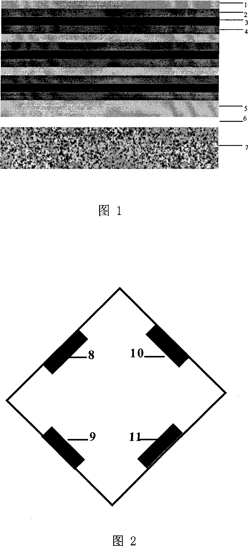
[0022] Stainless steel (1Cr18Ni9Ti) is cut after depositing the common TiAlN coating and the nanometer multi-layer coating of the present invention respectively with the cemented carbide blade whose grade is YG8 and model CNMG120408.
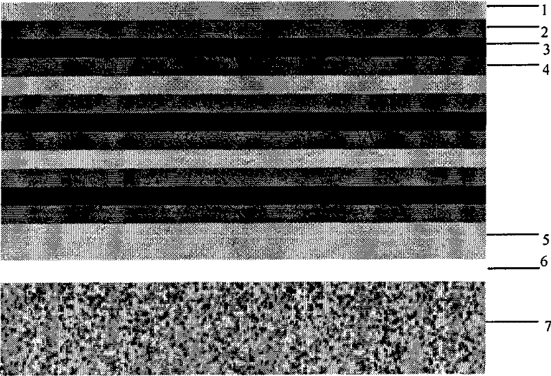
[0023] see figure 1 , the specific production process is as follows:
[0024] (A), cleaning the surface of the cemented carbide substrate 7;
[0025] (A'): Depositing a metal Ti layer 6 with a thickness of 20-30 nm and a transition layer 5 of 20-40 nm Ti N on the treated cemented carbide substrate 7;
[0026] (B), using 1 Ti target, 2 Ti x Al 1-x Target and 1 piece of Ti y Al 1-y target. During multi-target reactive magnetron sputtering, the placement positions of the four working targets are: Ti target and Ti target y Al 1-y The targets are respectively placed in positions 8 and 10 of the vacuum chamber, and two Ti x Al 1-x The targets are respectively placed in positions 9 and 11 of the vacuum chamber, and the vacuum degree of the va...
Embodiment 2
[0031] Stainless steel (1Cr18Ni9Ti) was milled after depositing common TiAlN coating and nanometer multi-layer coating of the present invention respectively with grade YG10 and model SEET12T3 cemented carbide inserts.
[0032] see figure 1 , the specific production process is as follows:
[0033] (A), cleaning the surface of the cemented carbide substrate 7;
[0034] (A): Depositing a metal Ti layer 6 with a thickness of 20-30 nm and a transition layer 5 of 20-40 nm TiN on the treated cemented carbide substrate 7;
[0035] (B), using 1 Ti target, 2 Ti x Al 1-x Target and 1 piece of Ti y Al 1-y target. During multi-target reactive magnetron sputtering, the placement positions of the four working targets are: Ti target and Ti target y Al 1-y The targets are respectively placed in positions 8 and 10 of the vacuum chamber, and two Ti x Al 1-x The targets are respectively placed in positions 9 and 11 of the vacuum chamber, and the vacuum degree of the vacuum chamber is hi...
PUM
| Property | Measurement | Unit |
|---|---|---|
| power | aaaaa | aaaaa |
| hardness | aaaaa | aaaaa |
| hardness | aaaaa | aaaaa |
Abstract
Description
Claims
Application Information
 - R&D
- Intellectual Property
- Life Sciences
- Materials
- Tech Scout
- Unparalleled Data Quality
- Higher Quality Content
- 60% Fewer Hallucinations
Browse by: Latest US Patents, China's latest patents, Technical Efficacy Thesaurus, Application Domain, Technology Topic, Popular Technical Reports.
© 2025 PatSnap. All rights reserved.Legal|Privacy policy|Modern Slavery Act Transparency Statement|Sitemap|About US| Contact US: help@patsnap.com


