Light emitting element, light emitting device and electronic apparatus
A technology of light-emitting devices and light-emitting layers, which is applied in the direction of electrical components, electric solid-state devices, circuits, etc., can solve problems such as the operation failure of light-emitting components, and achieve excellent effects in reducing unevenness and color
- Summary
- Abstract
- Description
- Claims
- Application Information
AI Technical Summary
Problems solved by technology
Method used
Image
Examples
Embodiment approach 1
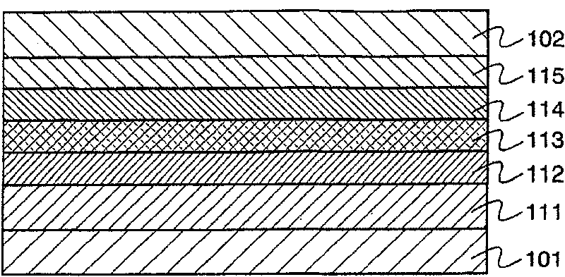
[0041] refer to figure 1 One mode of the light-emitting element of the present invention will be described.
[0042] figure 1 A light emitting element having a light emitting layer 113 between the first electrode 101 and the second electrode 102 is shown. exist figure 1 In the light emitting element shown, the mixed layer 111 is disposed between the light emitting layer 113 and the first electrode 101 . The hole transport layer 112 is disposed between the light emitting layer 113 and the mixing layer 111 , and the electron transport layer 114 and the electron injection layer 115 are disposed between the light emitting layer 113 and the second electrode 102 . In such a light-emitting element, when a voltage is applied to the first electrode 101 and the second electrode 102 so that the potential of the first electrode 101 is higher than the potential of the second electrode 102, holes are injected from the side of the first electrode 101 to emit light. In the layer 113, elec...
Embodiment approach 2
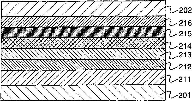
[0061] refer to figure 2 One mode of the light-emitting element of the present invention is described.
[0062] figure 2Shown is a light emitting element having a light emitting layer 213, a first mixed layer 215, and a second mixed layer 216 between the first electrode 201 and the second electrode 202, wherein the light emitting layer 213 is closer to the first electrode 201 than the first mixed layer 215 , the second mixed layer 216 is closer to the second electrode 202 than the first mixed layer 215 . In this light emitting element, the hole injection layer 211 and the hole transport layer 212 are provided between the light emitting layer and the first electrode 201 , and the electron transport layer 214 is provided between the light emitting layer 213 and the first mixed layer 215 . The first mixed layer 215 is a layer including an electron transport substance and one substance selected from alkaline metals, alkaline earth metals, alkaline metal oxides, alkaline earth ...
Embodiment approach 3
[0079] Next, one mode of the light-emitting element of the present invention will be described with reference to FIG. 20 . FIG. 20 shows a light emitting element having a plurality of light emitting layers, specifically a first light emitting layer 413a, a second light emitting layer 413b, and a third light emitting layer 413c between the first electrode 401 and the second electrode 402. This light-emitting element has a first mixed layer 421a and a second mixed layer 422a between the first light-emitting layer 413a and the second light-emitting layer 413b, and has a first mixed layer 421b between the second light-emitting layer 413b and the third light-emitting layer 413c. and the second mixed layer 422b. The first mixed layer 421a, 421b is a layer including an electron transport substance and a substance selected from alkaline metals, alkaline earth metals, alkaline metal oxides, alkaline earth metal oxides, alkaline metal fluorides, and alkaline earth metal fluorides. . T...
PUM
 Abstract
Description
Claims
Application Information


