Semiconductor materials and methods of producing them

A semiconductor and fuel component technology, applied in metal material coating process, thin material processing, coating and other directions, can solve the problems of strong electron amplification, difficult to manufacture diodes, and expensive to manufacture.

Inactive Publication Date: 2008-06-25
ATMOS (1998) LTD
View PDF1 Cites 8 Cited by
  • Summary
  • Abstract
  • Description
  • Claims
  • Application Information

AI Technical Summary

Problems solved by technology

Indeed, diodes are fragile and require encapsulation to protect them from atmospheric corrosion and mechanical damage
[0018] Also, they are expensive to manufacture and require complex and expensive production equipment utilizing highly toxic ma...

Method used


Image

  • Semiconductor materials and methods of producing them
  • Semiconductor materials and methods of producing them
  • Semiconductor materials and methods of producing them

Examples


Embodiment Construction

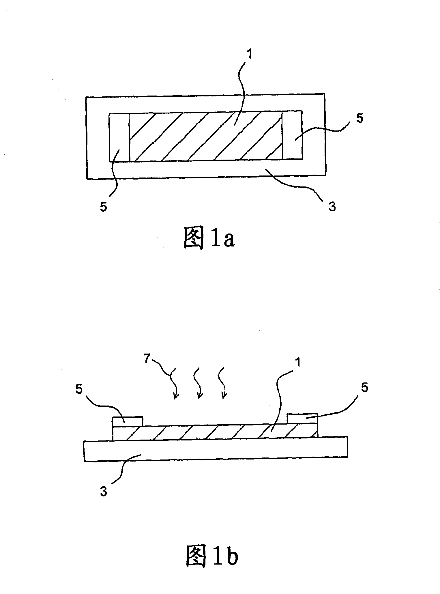
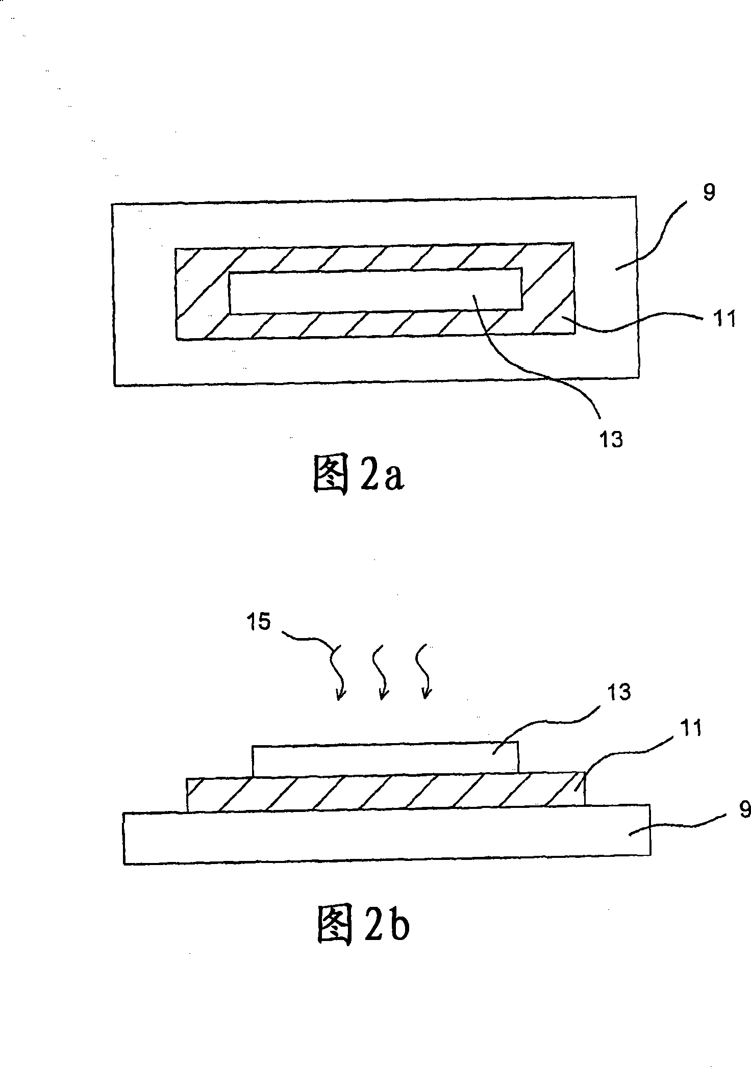
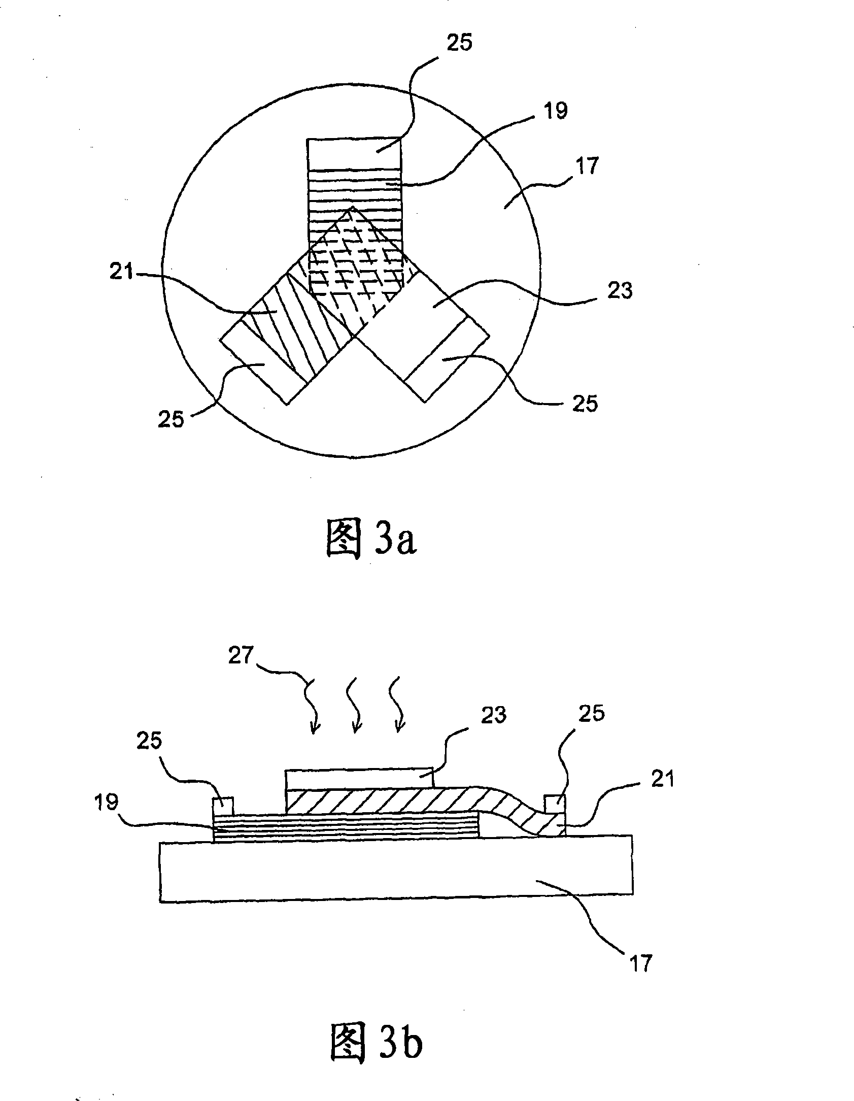
[0198] Figures 1-4 illustrate single-layer and multi-layer diode radiation detection devices, the general structure of which is known in the art, but is also an example of the structure of a radiation detection device according to an embodiment of the present invention.

[0199]FIG. 1 shows a single-layer wide bandgap detection device 1 on a substrate 3 . Contacts 5 are located at both ends of the single layer 1 . In use, a voltage is applied across the junction 5 such that a current is sensed in the external circuit when incident radiation 7 generates charge carriers within the monolayer 1 . In the prior art, the single layer 1 may be, for example, a NaI single crystal. In an embodiment of the present invention, the single layer 1 may be an n-type or p-type metal oxide, for example, a transition metal oxide. Preferably, the metal oxide particles have a metal core and an outer oxide shell, and more preferably have a degree of oxidation of 18 to 25 wt%.

[0200] The single l...


PUM

PropertyMeasurementUnit
Sizeaaaaaaaaaa
Resistanceaaaaaaaaaa
Melting pointaaaaaaaaaa

Abstract

A method of producing particles containing metal oxide for use in semiconductor devices includes the steps of heating metal-containing particles in a flame produced by a mixture of oxygen and a fuel component comprising at least one combustible gas selected from hydrogen and hydrocarbons, the oxygen being present in the mixture in a proportion of not less than 10 mole% below, and not more than 60 mole% above, a stoichiometric amount relative to the fuel component, so as to oxidize metal in at least an outer shell of the particles; cooling the oxidized particles by feeding them into a liquid or sublimable solid medium; collecting the cooled oxidized particles; and providing a distance between entry of the particles into the flame and collection of the particles of at least 300mm. In this manner, such particles may be oxidized so as to provide a shell of metal oxide material which leaving unoxidized a core of metal. A semiconductive layer of such particles on a substrate may be formed by feeding, to a hot zone, such preoxidized metal-containing particles; heating the metal-containing particles in the hot zone to render the particles at least partially molten; and depositing the particles in the at least partially molten state onto the substrate. The above oxidation process may be employed to provide metal oxide particles in which different respective metals having different respective valencies are present in different respective molar proportions. The valencies and molar proportions may be selected so as to provide n- or p-type semiconductor layers.

Description

technical field [0001] The present invention relates to semiconductor materials, in particular semiconductor materials made of metal oxides, especially transition metal oxides, and methods for the manufacture of these semiconductor materials. [0002] The invention also relates to devices for detecting radiation comprising ionizing radiation, electromagnetic radiation and nuclear radiation such as neutron radiation, in particular comprising radiation detecting semiconductor materials made of metal oxides. Background technique [0003] Conventional radiation detection devices include scintillation devices such as Geiger counters and ionization chambers. A diatomic gas is contained within a low pressure chamber, and the chamber has two junction areas to which a voltage is applied. [0004] The effect of the radiation causes the low pressure diatomic gas to dissociate / ionize, and the ions are attracted to the respective junction areas where they discharge. The discharge rate ...

Claims


Application Information

Patent Timeline
IPC IPC(8): C23C8/10C23C4/10B22F1/16C01G1/02C23C4/12
CPCC23C4/124Y10T428/256C01P2002/72B22F2998/00B22F1/02C01G1/02Y10T428/2998C23C4/105C23C8/10Y10T428/254Y10T428/2982B22F3/115Y10T428/2991C23C4/11C23C4/129B22F1/16B22F2201/03C01G31/02C01G37/033C01G45/02C01G49/02C01G49/06C01G51/04C01G53/04
Inventor 杰弗里·博阿德曼
Owner ATMOS (1998) LTD
Why Eureka
Try Eureka