Multi-test point semiconductor test machine station automated setting method

A technology of testing machine and setting method, applied in semiconductor/solid-state device testing/measurement, digital circuit testing, electronic circuit testing, etc. problems, to reduce risks and losses, reduce test costs, and improve detection accuracy and efficiency

Inactive Publication Date: 2008-07-02
CHROMA ELECTRONICS SHENZHEN
View PDF0 Cites 21 Cited by
  • Summary
  • Abstract
  • Description
  • Claims
  • Application Information

AI Technical Summary

Problems solved by technology

The disadvantages of this testing method are:
[0008] On the one hand, every time the production line is started, the operator needs to set the state parameters of each test base 11 by the central control module 10, and the same is true for changing the production line. Difficulties in management also make it difficult to improve test efficiency
[0009] On the other hand, after the frequent testing of the power-on/off process, the hard disks of each test base 11 are prone to problems or even damage. Whether the operator swaps the hard disks of the two test bases or updates the damaged hard disk, it is necessary to update the hard disk. Content, a little carelessness will cause the test program to be inconsistent or not corresponding to the tested product, which will affect the correctness of the updated test results
If you mistakenly test a qualified product as a substandard product, you will only lose one I

Method used


Image

  • Multi-test point semiconductor test machine station automated setting method
  • Multi-test point semiconductor test machine station automated setting method
  • Multi-test point semiconductor test machine station automated setting method

Examples


Embodiment Construction

[0033] The aforementioned and other technical contents, features and effects of the present invention will be clearly presented in the following detailed description of the preferred embodiments given in conjunction with the accompanying drawings.

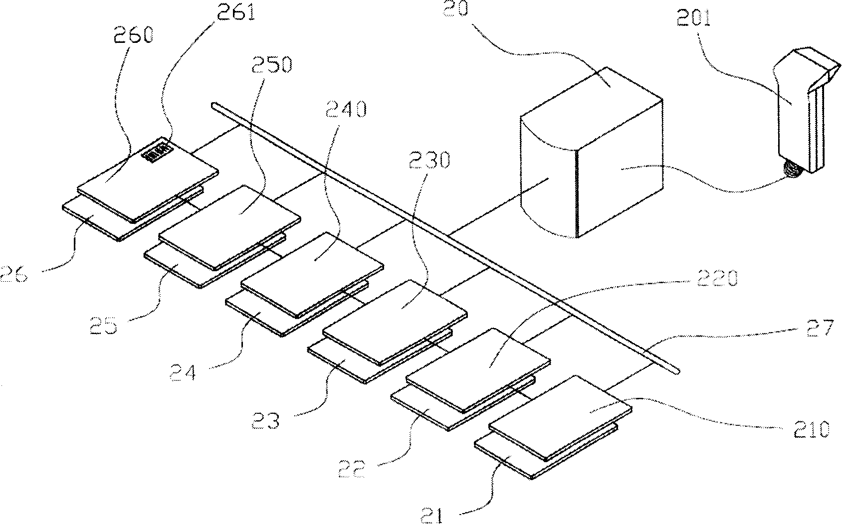
[0034] see figure 2 , as a preferred embodiment of the automatic setting method of the multi-test port semiconductor test machine of the present invention, the test machine includes a control device 20, a bar code reading device 201, six test bases 21-26, and Six test circuit boards 210-260 respectively arranged on the test bases 21-26, and each test circuit board has an identification code; wherein, the control device 20 is connected to the test bases 21-26 via the internal LAN 27 The test circuit boards 210-260 of the control device 20 are also provided with an identification code obtaining device.

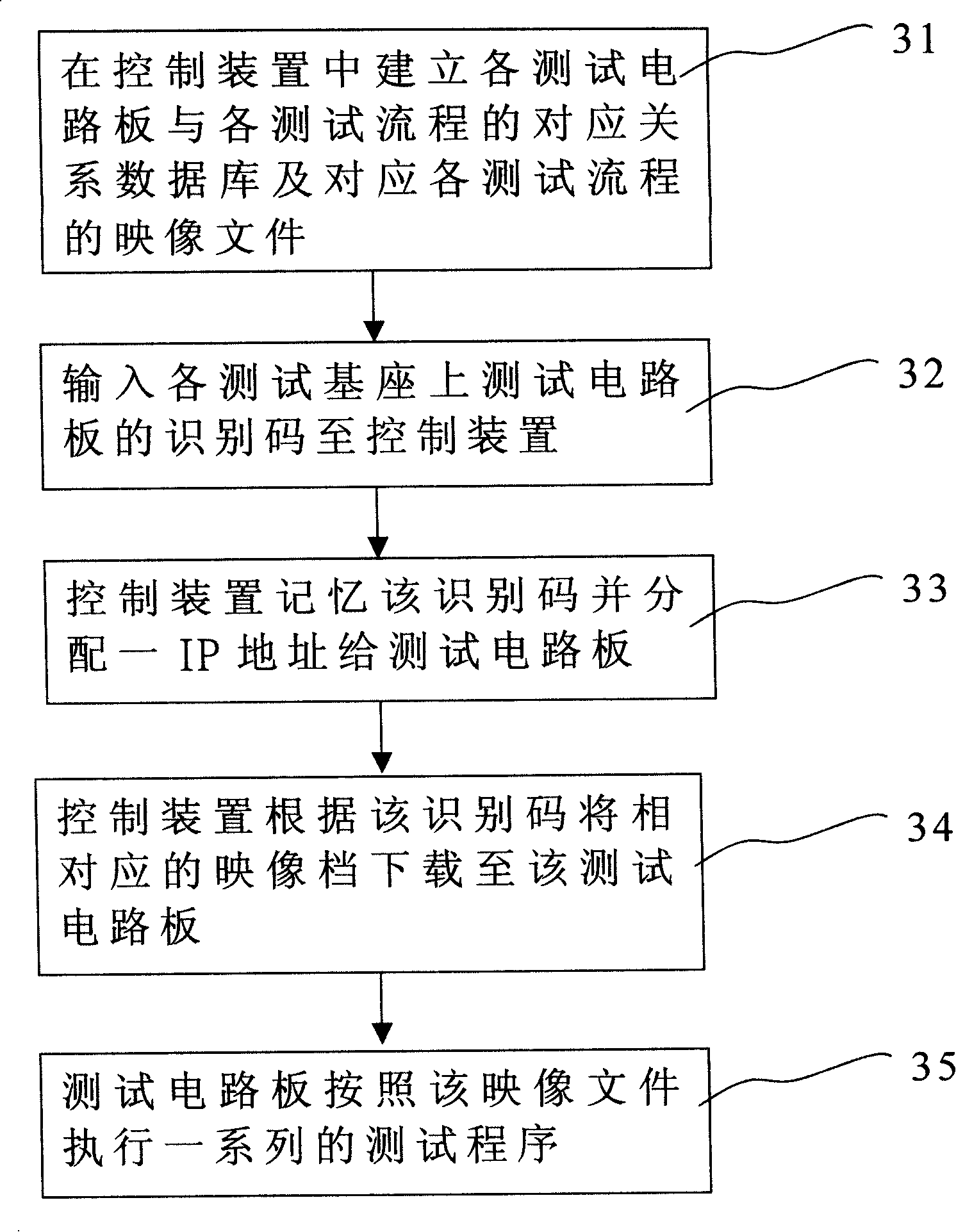
[0035] Such as image 3 As shown, before the test machine actually starts to operate, firstly, in the machine building step 31, ...


PUM


Abstract

An automatic setting method for a multi-ports semiconductor test apparatus for different test products comprises the following steps of: making the complicated steps of test procedure, information of test products and parameters' setting of the apparatus into corresponding image files respectively corresponding to the test products so that the image file is managed by the test apparatus; inputting the identity code on each to-be-tested plate before the product test to start the a series of automatic test procedures. The method can greatly reduce the complicated setting before the product test so as to further ensure the correctness and integrity, and greatly improving the effectiveness of management and efficiency of product test.

Description

Technical field: [0001] The present invention relates to an automatic setting method of a multi-test port semiconductor test machine, in particular to a method in which each test base can be powered on remotely to perform automatic testing without installing a hard disk, an optical drive or a floppy drive. Background technique: [0002] Integrated circuit (IC) components have become the indispensable core of almost all electronic equipment, so the reliability of IC has undoubtedly become an extremely important link in determining the reliability of electronic equipment. [0003] At present, the automated test machines used to test ICs can be roughly divided into three types: the test base provides simulated signals and captures the output signals of each output pin for simulated tests; A real-world test that puts the IC under test into an actual use environment. [0004] Although the simulation test can obtain the complete electrical characteristics of the IC to be tested, ...

Claims


Application Information

Patent Timeline
IPC IPC(8): G01R31/28G01R31/303G01R31/317G01R31/3185G01R31/00G06F11/00G06F17/00G05B19/04H01L21/66
Inventor 龚汉忠赖佳宏
Owner CHROMA ELECTRONICS SHENZHEN
Why Eureka
Try Eureka