Method for cleaning cavity of semiconductor etching equipment

An etching equipment and semiconductor technology, applied in cleaning methods and appliances, semiconductor/solid-state device manufacturing, chemical instruments and methods, etc., can solve problems such as impact, etching process drift, and product yield reduction

Active Publication Date: 2008-07-09
BEIJING NAURA MICROELECTRONICS EQUIP CO LTD
View PDF0 Cites 14 Cited by
  • Summary
  • Abstract
  • Description
  • Claims
  • Application Information

AI Technical Summary

Problems solved by technology

[0009] (1) The accumulation of deposits makes the chamber environment constantly change during the process, which affects process parameters such as etch rate and uniformity, resulting in the drift of the etching process
[0010](2) Deposit cracking will generate a large number of particles in the reaction chamber, which will significantly reduce th

Method used


Image

  • Method for cleaning cavity of semiconductor etching equipment
  • Method for cleaning cavity of semiconductor etching equipment
  • Method for cleaning cavity of semiconductor etching equipment

Examples


Embodiment 1

[0036] The cleaning method of the chamber of the semiconductor etching equipment described in the present invention does not require special equipment, and can be completed by using the equipment in the prior art. Using the existing cleaning method, the process parameters are set to the range required by the present invention And can reach the effect of the present invention.

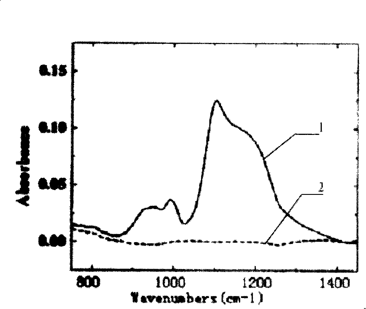
[0037] Using ClF 3 and He according to the volume ratio of 1:1 mixed gas, because ClF 3 With strong reactivity, it can react with all substances in the deposit under normal temperature and non-plasma conditions to generate volatile fluoride or chloride, which is discharged through the vacuum system to achieve the purpose of cleaning the chamber. Simultaneously ClF 3 It can also react with the surface of the metal chamber wall to form a dense metal fluoride surface layer, which prevents further contact between the gas and the inner wall of the metal chamber, and realizes the protection of the inner wal...

Embodiment 2

[0041] Concrete operation step is carried out by embodiment 1, and process parameter is as follows:

[0042] Inert gas is Ar, ClF 3 And Ar volume ratio is 0.01:1, ClF 3 The flow rate of the mixed gas composed of Ar and Ar is 10 sccm, and the chamber pressure in the chamber of the semiconductor etching equipment is 5 mT.

Embodiment 3

[0044] Concrete operation step is carried out by embodiment 1, and process parameter is as follows:

[0045] The inert gas is Ne, ClF 3 and Ne volume ratio is 99.9:1, ClF 3 The flow rate of the mixed gas composed of Ne and Ne is 100 sccm, and the chamber pressure in the chamber of the semiconductor etching equipment is 500 mT.


PUM


Abstract

The invention relates to a method for cleaning the chamber of a semiconductor etching equipment. The procedures of the method are as follows: mixed gas composed of CIF3 and inert gas is used for cleaning the chamber of a semiconductor etching equipment. The inert gas or O2 or the mixed gas composed of the inert gas and O2 is used for cleaning the chamber of a semiconductor etching equipment. The method of the invention can attain the aim of cleaning the chamber of the semiconductor etching equipment on condition of non-plasma starting. The method can effectively prolong the service life of the part, reduce the number of metal particle and improve the yield rate of product. In addition, the method does not require plasma starting during the cleaning process, with the result that the cost of ownership can be further reduced during the processing of wafer.

Description

technical field [0001] The invention relates to a cleaning method for a chamber, in particular to a cleaning method for a semiconductor etching equipment chamber. Background technique [0002] Etching refers to the process of removing unnecessary parts from the wafer by physical or chemical methods in the integrated circuit manufacturing process. It is usually divided into two categories: wet etching and dry etching. Among them, wet etching refers to the method of etching by using liquid chemical reagents or solutions through chemical reactions; while dry etching mainly uses low-voltage discharge to produce etching. The ions or radicals of the plasma achieve the purpose of etching materials through physical effects such as bombardment or chemical reactions. [0003] Plasma etching is one of the key processes in integrated circuit manufacturing. Its purpose is to completely copy the mask pattern to the surface of the silicon wafer. Etching and etching of Via and Trench. No...

Claims


Application Information

Patent Timeline
IPC IPC(8): B08B7/00H01L21/00H01L21/3065
Inventor 付春江
Owner BEIJING NAURA MICROELECTRONICS EQUIP CO LTD
Why Eureka
Try Eureka