

Method for forming graphic pattern
A patterning and patterning technology, which is applied in the field of pattern formation in the step of forming fine patterns in the manufacturing method, can solve problems such as damage, poor process results, and inability to provide a protective lower layer.
- Summary
- Abstract
- Description
- Claims
- Application Information
AI Technical Summary
Problems solved by technology
Method used
Image

Examples
Embodiment Construction
[0021] see Figure 3 to Figure 9 , which shows a schematic cross-sectional view of a specific embodiment of the pattern forming method of the present invention, wherein the same elements or parts are still represented by the same symbols. It should be noted that the drawings are for illustration purposes only and are not drawn to original scale.
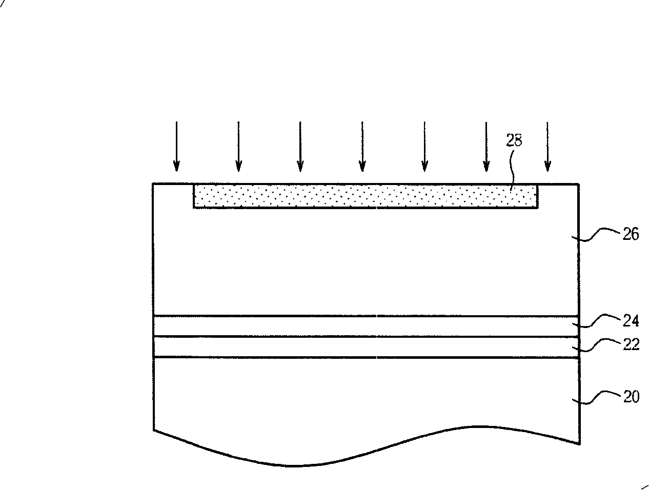
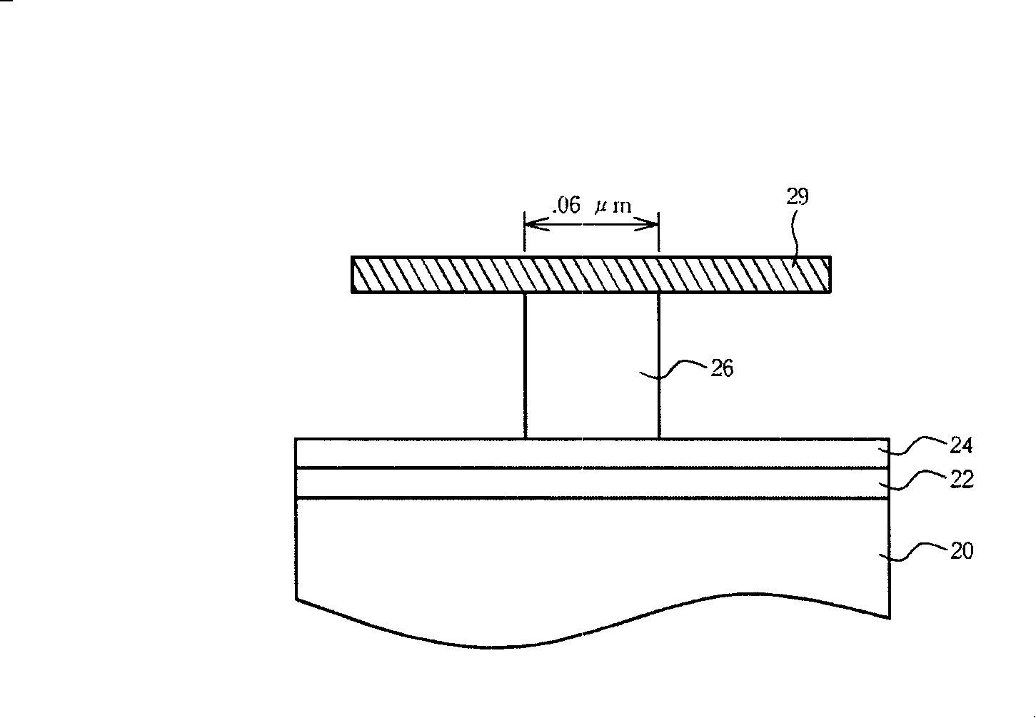
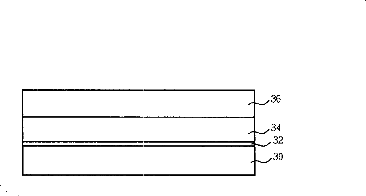
[0022] First, a substrate is provided, which may include an insulating layer, a conductive layer, or other layers to be patterned, such as silicon, aluminum, indium tin oxide, molybdenum, silicon dioxide, doped silicon dioxide, silicon nitride , tantalum, copper, polysilicon, ceramics, aluminum / copper mixtures, various polymer resins, etc., but not limited thereto. There is a layer to be etched on the substrate. Such as image 3 As shown, in this specific embodiment, the substrate includes a silicon substrate 30 and a gate dielectric layer 32 and a polysilicon layer 34 thereon as layers to be etched. A first resist layer 36 is fo...
PUM
 Abstract
Description
Claims
Application Information