Semiconductor light emitting device and method for fabricating same

一种发光器件、半导体的技术,应用在半导体器件、半导体激光器、半导体/固态器件零部件等方向,能够解决妨碍膜中Mg活化、受主浓度和空穴密度减少等问题,达到抑制增加、抑制元件操作电压、抑制扩散的效果

Active Publication Date: 2008-07-16
SHARP FUKUYAMA LASER CO LTD
View PDF1 Cites 3 Cited by
  • Summary
  • Abstract
  • Description
  • Claims
  • Application Information

AI Technical Summary

Problems solved by technology

This hampers the activation of Mg in the film, which causes a decrease in acceptor concentration and hole density

Method used


Image

  • Semiconductor light emitting device and method for fabricating same
  • Semiconductor light emitting device and method for fabricating same
  • Semiconductor light emitting device and method for fabricating same

Examples


example 1

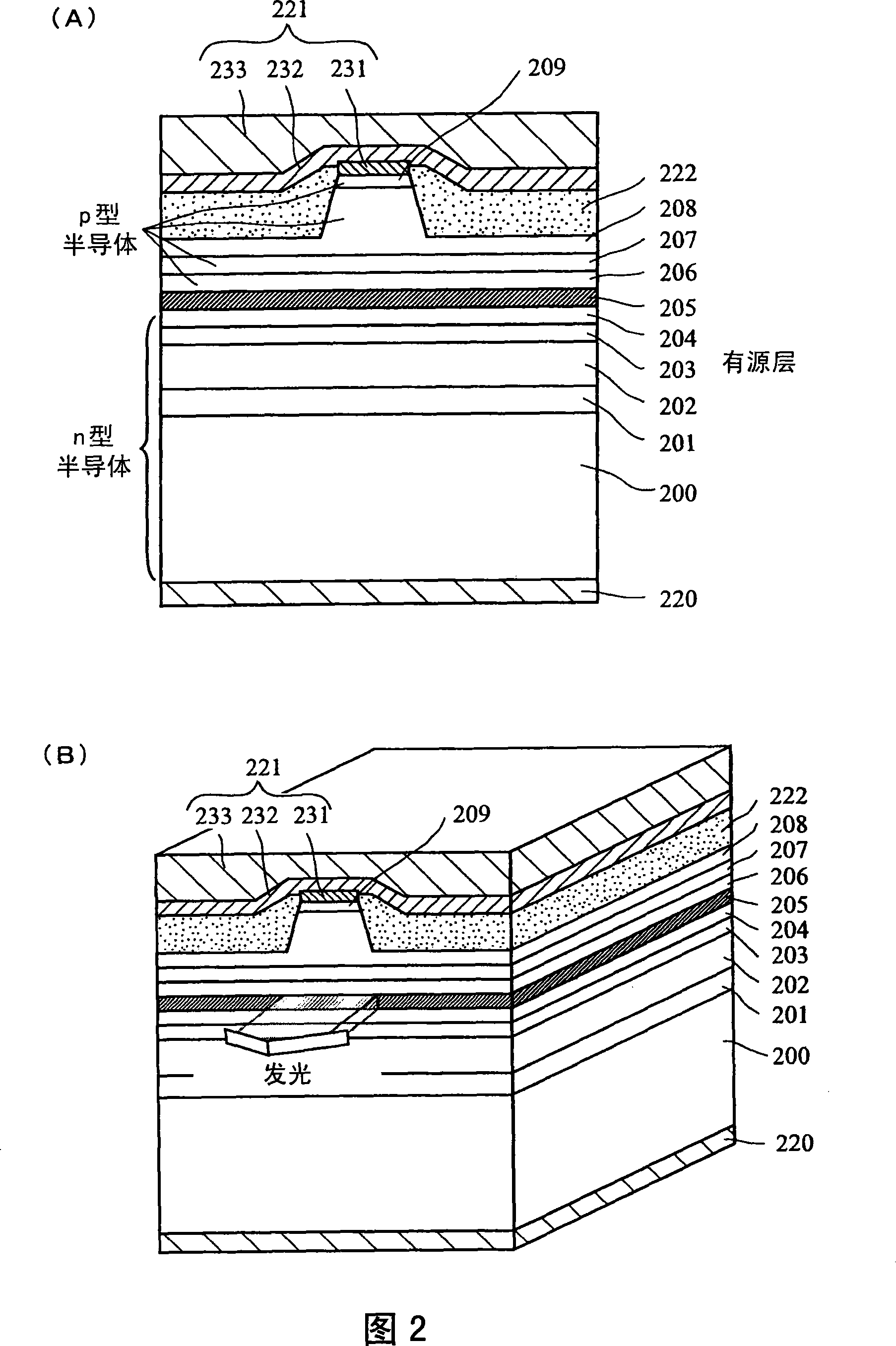
[0051] 2(A) is a schematic sectional view of a semiconductor laser element of the semiconductor laser device used in Example 1 according to the present invention.

[0052] The insulating layer 222 is disposed on the periphery of the protruding portion of the ridge structure to form a current confinement path structure having one electrode electrically connected only to the top of the protruding portion, thereby limiting the portion through which current passes. The current limiting path structure enables approximate control of the spot shape of the emitted light. The insulating layer 222 consists of 1 x 10 17 / cm 3 or above concentrations of hydrogen atoms. The width of the protruding portion of the ridge structure is approximately 1.6 μm, and the length of the resonant cavity is 600 μm. The element undergoes an AR (anti-reflection) coating on the front side and a HR (high reflection) coating on the back side.

[0053] The P-type conductive layer is doped with from 1×10 1...

example 2

[0084] A method and assembly equipment for manufacturing a nitride semiconductor laser device according to the present invention will be described.

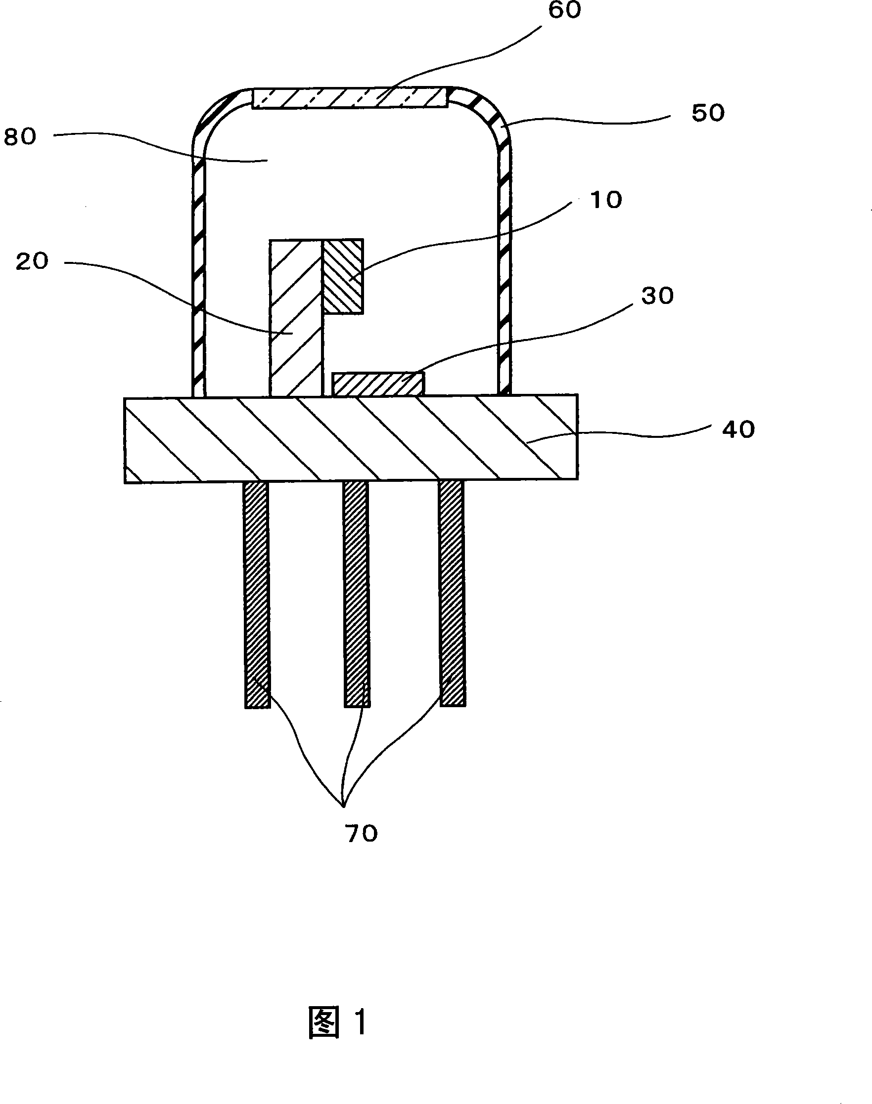
[0085] Referring to FIG. 10 , the assembly device has a front chamber 101 and a working chamber 102 . The front chamber 101 makes it possible to introduce the necessary components for assembly into the working chamber 102 without opening the working chamber 102 to the atmosphere. For this purpose, the front chamber 101 has means 103 for introducing purge gas. The working chamber 102 has therein an assembly mechanism 104 for assembling the nitride semiconductor laser device, thereby enabling the assembly work to be performed in an externally isolated sealed space. Between the front chamber 101 and the working chamber 102 there is a transfer device (not shown) for transferring the necessary components required for assembly. The front chamber 101 and the working chamber 102 are separated by a door 109 .

[0086] The working chamb...


PUM


Abstract

A nitride semiconductor device includes a stem. A heat sink is provided on the stem. At least one nitride semiconductor light-emitting element is connected to the heat sink. A light-detecting element for detecting light from the semiconductor light-emitting element is provided on the stem. A cap for encapsulating therein the heat sink, the semiconductor light-emitting element, and the light-detecting element in a sealed manner is connected to the stem. The space in the cap has an encapsulated atmosphere. The encapsulated atmosphere contains a component for inhibiting diffusion of hydrogen atoms contained in the semiconductor light-emitting element. The present invention suppresses defect due to an increase in operation voltage to increase a ratio of good goods thereby improving the fabrication yield of the semiconductor light-emitting device.

Description

technical field [0001] The present invention relates generally to a semiconductor light emitting device, and more particularly to a semiconductor light emitting device improved to suppress defects due to an increase in operating voltage. The invention also relates to a method for manufacturing such a semiconductor light emitting device. Background technique [0002] Group III nitride semiconductor laser elements have a wide oscillation wavelength from ultraviolet light to visible light, and are attracting attention as short-wavelength light sources suitable for high-density optical storage media. In addition to optical recording media, Group III nitride semiconductor laser elements are expected as visible light sources such as lamps and backlights. For a wider range of applications, technologies have been developed that target the operational reliability of nitride semiconductor laser elements while improving light emission output. [0003] FIG. 11(A) is a sectional view o...

Claims


Application Information

Patent Timeline
Patent Type & Authority Applications(China)
IPC IPC(8): H01S5/022H01S5/026H01S5/024H01S5/22H01S5/00H01L33/00H01L23/00H01S5/223
CPCH01L31/0203H01L31/18H01S5/02224H01S5/3063H01S5/02212H01L31/143H01S5/2231H01S5/0021H01S5/2222B82Y20/00H01S5/0683H01S5/0425H01S5/34333
Inventor 高谷邦启花冈大介石田真也
Owner SHARP FUKUYAMA LASER CO LTD
Why Eureka
Try Eureka