LED with high efficiency and method for manufacturing the same

A technology for light-emitting diodes and a manufacturing method, which is applied to electrical components, circuits, semiconductor devices, etc., can solve the problems of increasing the opaque area and decreasing the brightness of light-emitting diode components.

Active Publication Date: 2011-10-12
EPISTAR CORP
View PDF5 Cites 0 Cited by
  • Summary
  • Abstract
  • Description
  • Claims
  • Application Information

AI Technical Summary

Problems solved by technology

However, since the electrodes are opaque, the increase in the area of ​​the electrodes will lead to an increase in the opaque area, resulting in a decrease in the luminous brightness of the LED assembly.

Method used


Image

  • LED with high efficiency and method for manufacturing the same
  • LED with high efficiency and method for manufacturing the same
  • LED with high efficiency and method for manufacturing the same

Examples


Embodiment Construction

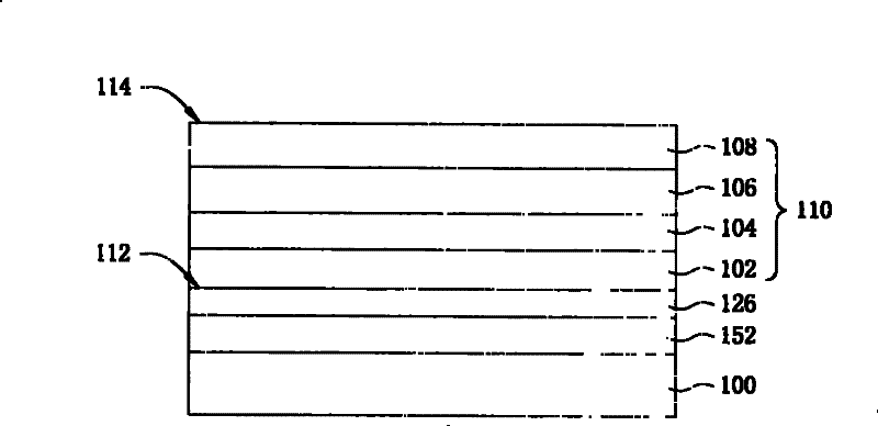
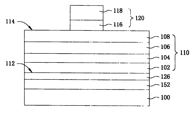
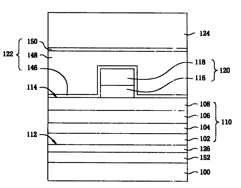
[0032] The invention proposes a high-efficiency light-emitting diode, which can improve the light-emitting brightness of the light-emitting diode assembly, and can improve the operation reliability and stability of the light-emitting diode assembly. In order to make the description of the present invention more detailed and complete, reference may be made to the following descriptions and Figure 1 to Figure 8 icon of the .

[0033] Please refer to Figure 1 to Figure 8 , which is a process cross-sectional view of a high-efficiency light-emitting diode according to a preferred embodiment of the present invention. In an exemplary embodiment of the present invention, when manufacturing the light emitting diode device, the growth substrate 100 is firstly provided, and then the etch stop layer 152 is directly grown on the surface of the growth substrate 100 by, for example, deposition. Next, a first electrical ohmic contact layer 126 is formed on the etch stop layer 152 , wherein ...


PUM


Abstract

The invention discloses a high efficiency luminescence diode and a method for preparation. The high efficiency luminescence diode at least comprises a permanent base plate, a first and a second contacting metal layers, a junction layer, a diffusion barrier layer, a reflection metal layer, a transparent conductive oxide layer, a luminescence extension structure and an electrical second composite electrode pad, wherein the first and the second contacting metal layers are respectively arranged on two relative surfaces of the permanent base plate, the junction layer is arranged on the second contacting metal layer, the diffusion barrier layer is arranged on the junction layer, and the permanent base plate, the junction layer and the diffusion barrier layer are capable of conducting. The reflection metal layer is arranged on the diffusion barrier layer, the transparent conductive oxide layer is arranged on the reflection metal layer, the luminescence extension structure is arranged on the transparent conductive oxide layer and is equipped with a first and a second surfaces, and a second electrical composite electrode pad is arranged on the second surface of the luminescence extension structure.

Description

technical field [0001] The invention relates to a light-emitting diode (LED) and a manufacturing method thereof, in particular to a high-efficiency light-emitting diode and a manufacturing method thereof. Background technique [0002] In the production of light-emitting diodes, III-V semiconductor compounds, such as gallium phosphide (GaP), gallium arsenic phosphide (GaAsP), gallium indium phosphide (GaInP), aluminum gallium arsenide (AlGaAs) or aluminum gallium phosphide (AlGaP) and aluminum gallium indium phosphide (AlGaInP) are quite common materials. Generally, the conventional light-emitting diode structure uses N-type gallium arsenide (GaAs) as the growth substrate (Growth Substrate) material. Since the growth substrate made of N-type gallium arsenide absorbs light, among the photons generated in the active layer of the light-emitting diode, most of the photons towards the growth substrate will be absorbed by the growth substrate, which seriously affects the performan...

Claims


Application Information

Patent Timeline
Patent Type & Authority Patents(China)
IPC IPC(8): H01L33/00H01L33/02
Inventor 洪详竣
Owner EPISTAR CORP
Why Eureka
Try Eureka