Device and method for measuring metal film stress evolution when loading current

A metal thin film, a technique for measuring current

Inactive Publication Date: 2008-08-06
山东云度材料科技有限公司
View PDF0 Cites 9 Cited by
  • Summary
  • Abstract
  • Description
  • Claims
  • Application Information

AI Technical Summary

Problems solved by technology

Taking copper thin film as an example, usually the copper thin film at room temperature is in a state of residual tensile stress, and the diffraction peak is located on the left side of the standard peak. When a direct current is passed through the film, the diffraction peak shifts to the left. To the right of the standard peak, the grazing incidence XRD test results can qualitatively indicate that the stress in the film changes from a tensile stress state to a compressive stress state with the increase of the current, but there is no way to accurately quantitatively measure the stress change of the film, and the atomic force microscope can also The thermal strain is calculated by the displacement of the film, but many influencing factors must be removed in the measurement and analysis process, such as the current interference that the cantilever beam of the atomic force microscope will receive

Method used


Image

  • Device and method for measuring metal film stress evolution when loading current
  • Device and method for measuring metal film stress evolution when loading current
  • Device and method for measuring metal film stress evolution when loading current

Examples


Embodiment 1

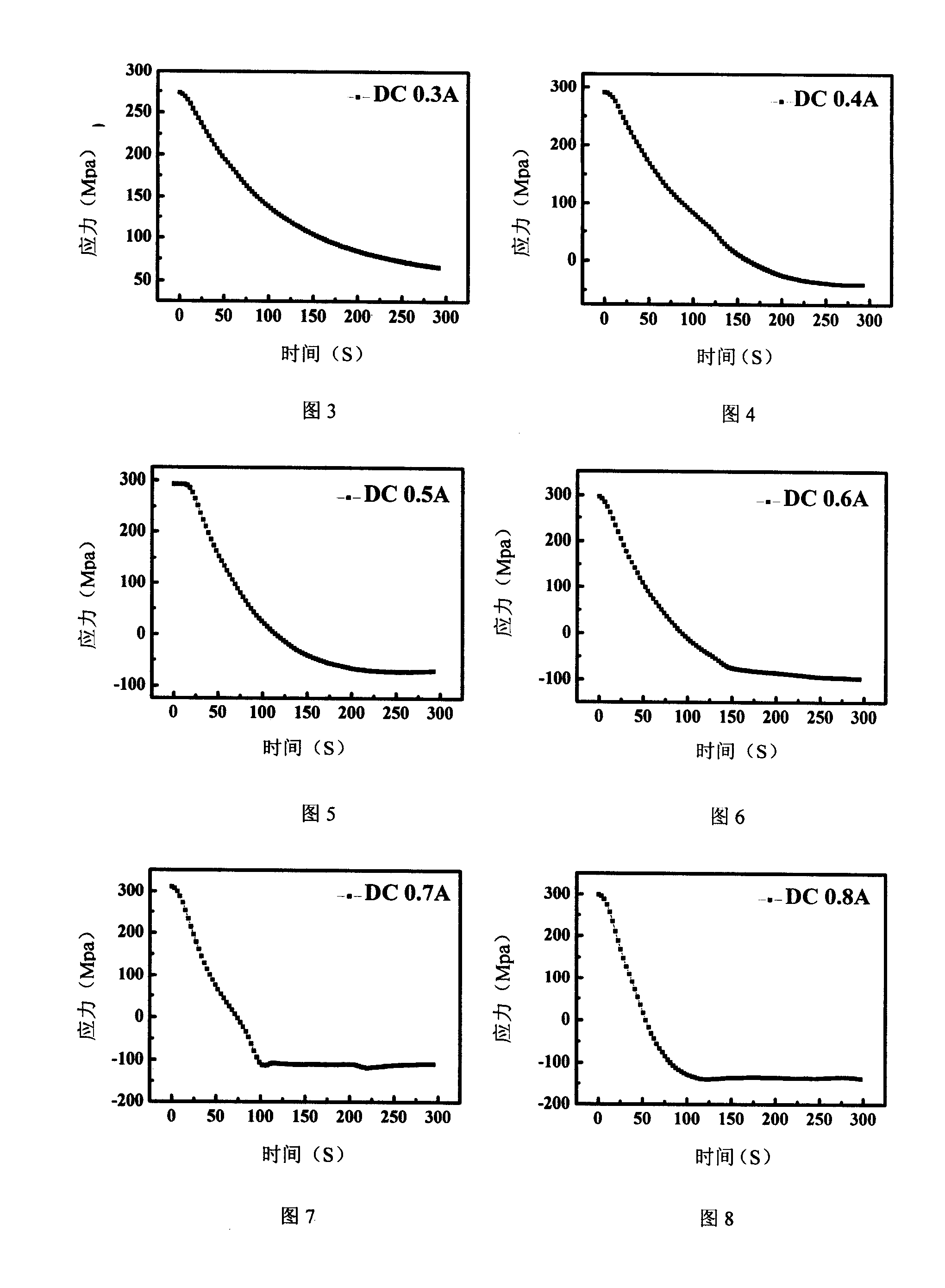
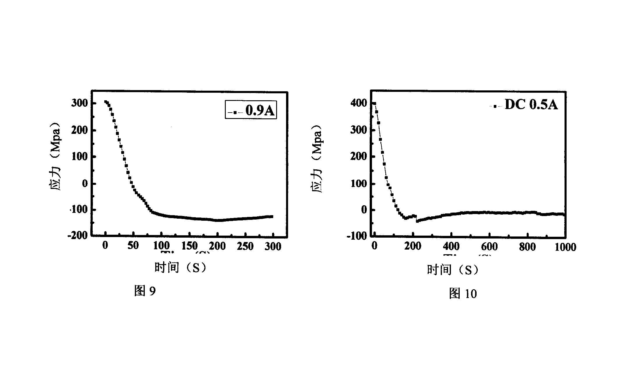
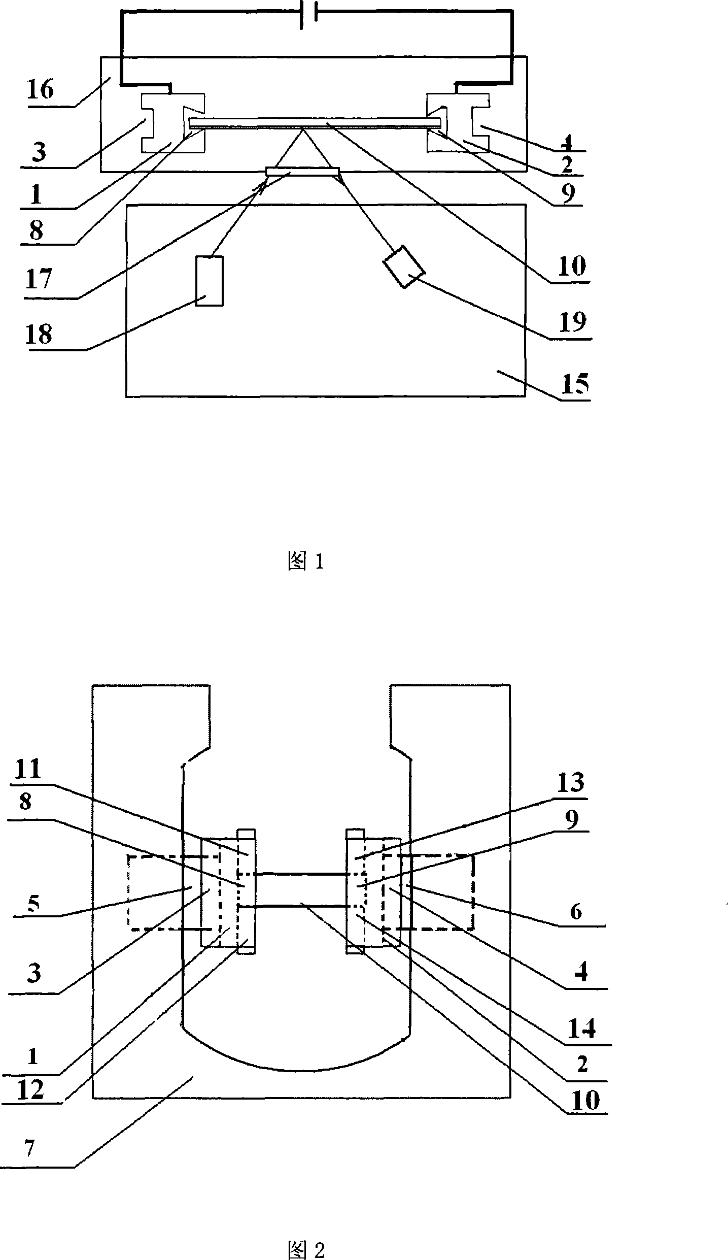
[0040] Embodiment 1: adopt magnetron sputtering deposition method that copper thin film is deposited on 2 inches thermally oxidized silicon chip: SiO2(50nm) / Si(380 μm) / SiO2(50nm), copper thin film thickness 1 μm, deposition process parameter is : sputtering power 100W; sputtering bias -80V; background vacuum: 1.0×10 -6 Pa; Working air pressure (Ar) 0.1Pa; Use a diamond scriber to cut it into a rectangular metal film sample 10 of 5mm * 15mm, place the rectangular metal film sample 10 from the first metal material placement table 1 underside and the second The lower side of the metal material placement table 2 is put into, the first metal plug 11 is inserted into the upper side of the first dovetail-shaped through groove 8, the second metal plug 12 is inserted into the lower side of the first dovetail-shaped through groove, and the second metal plug 12 is inserted into the lower side of the first dovetail-shaped through groove Three metal plugs 13 are inserted into the upper sid...

Embodiment 2

[0041] Embodiment 2: adopt magnetron sputtering deposition method to deposit copper thin film on 2 inches thermally oxidized silicon wafer: SiO2(50nm) / Si(380 μm) / SiO2(50nm), copper thin film thickness 1 μm, deposition process parameter is : sputtering power 100W; sputtering bias -80V; background vacuum: 1.0×10 -6 Pa; Working air pressure (Ar) 0.1Pa; Use a diamond scriber to cut it into a rectangular metal film sample 10 of 5mm * 15mm, place the rectangular metal film sample 10 from the first metal material placement table 1 underside and the second The lower side of the metal material placement table 2 is put into, the first metal plug 11 is inserted into the upper side of the first dovetail-shaped through groove 8, the second metal plug 12 is inserted into the lower side of the first dovetail-shaped through groove, and the second metal plug 12 is inserted into the lower side of the first dovetail-shaped through groove Three metal plugs 13 are inserted into the upper side of t...

Embodiment 3

[0042] Embodiment 3: adopt magnetron sputtering deposition method to deposit copper thin film on 2 inches thermally oxidized silicon wafer: SiO2(50nm) / Si(380 μm) / SiO2(50nm), copper thin film thickness 1 μm, deposition process parameter is : sputtering power 100W; sputtering bias -80V; background vacuum: 1.0×10 -6 Pa; Working air pressure (Ar) 0.1Pa; Use a diamond scriber to cut it into a rectangular metal film sample 10 of 5mm * 15mm, place the rectangular metal film sample 10 from the first metal material placement table 1 underside and the second The lower side of the metal material placement table 2 is put into, the first metal plug 11 is inserted into the upper side of the first dovetail-shaped through groove 8, the second metal plug 12 is inserted into the lower side of the first dovetail-shaped through groove, and the second metal plug 12 is inserted into the lower side of the first dovetail-shaped through groove Three metal plugs 13 are inserted into the upper side of t...


PUM

PropertyMeasurementUnit
thicknessaaaaaaaaaa
thicknessaaaaaaaaaa
thicknessaaaaaaaaaa

Abstract

The invention discloses a device and a method for measuring the stress evolution in a metallic thin film when a current is loaded. A sample placing device is provided, and current loading is realized through the wire contact between the metallic thin film and the sample placing device. A metallic thin film sample is placed in a dovetail-shaped groove in a metallic material placing platform, the metallic thin film sample is in wire contact with metallic placing platform by gravity to ensure that the metallic thin film and the metallic placing platform are conductive, the Joule heat and the electric creep curvature of the metallic thin film change when the current is applied, and then a plurality of laser stress measurement devices are used to measure the stress evolution in the metallic thin film when the current is loaded. No external force is applied on the thin film sample to realize in-situ measurement of the stress evolution in the metallic thin film when the current is loaded and consequently analyzes the creep deformation behavior of the metallic thin film in a heat/force/electricity multiple coupling field. The method has the advantages of simplicity, accuracy, etc.

Description

technical field [0001] The invention relates to metal thin film materials, belonging to the field of thin film materials, in particular to a device and method for measuring stress evolution in a metal thin film when current is applied. Background technique [0002] Widely used in metal thin film materials (such as Cu) in VLSI and micron-scale device materials in microelectromechanical systems (MEMS), during the preparation and use of micromachining, due to the difference between the thin film material and its surrounding materials The coefficient of thermal expansion is different. Due to the power-on and power-off and the action of the electric pulse signal, accompanied by temperature cycles, the film material will experience the effect of cyclic thermal stress. Usually, the film material works under higher stress and higher temperature, and creep deformation is related to it. An important issue of membrane reliability in service. The research on thermomechanical behavior b...

Claims


Application Information

Patent Timeline
Patent Type & Authority Applications(China)
IPC IPC(8): G01N33/00G01N25/26G01N3/28
Inventor 孙军王章洁刘刚孙冰丁向东江峰
Owner 山东云度材料科技有限公司
Why Eureka
Try Eureka