Non-volatile memory and its manufacturing method

A non-volatile, manufacturing method technology, applied in semiconductor/solid-state device manufacturing, electric solid-state devices, semiconductor devices, etc., can solve the problem of slow operation speed of storage units, low reading current of storage units, failure to improve component performance, etc. problem, to achieve the effect of reducing the size of the memory cell, large read current, and avoiding electrical penetration

Inactive Publication Date: 2008-09-24
POWERCHIP SEMICON CORP
View PDF0 Cites 5 Cited by
  • Summary
  • Abstract
  • Description
  • Claims
  • Application Information

AI Technical Summary

Problems solved by technology

[0006] However, the program of writing and reading the memory cells in the NAND array is more complicated, and because many memory cells are connected in series in the array, the read current of the memory cells is small, and the The problem that causes the operation speed of the memory cell to slow down and cannot improve the performance of the device

Method used


Image

  • Non-volatile memory and its manufacturing method
  • Non-volatile memory and its manufacturing method
  • Non-volatile memory and its manufacturing method

Examples


Embodiment Construction

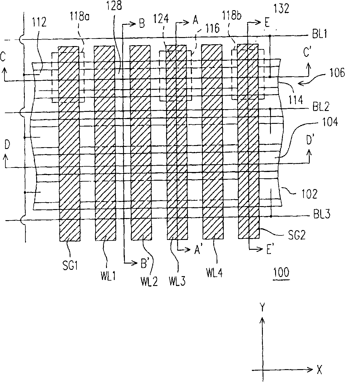
[0095] Figure 1A What is shown is a top view of a preferred embodiment of the non-volatile memory of the present invention. Figure 1B for depicted as Figure 1A Structural cross-section along line A-A'. Figure 1C for depicted as Figure 1A The structural cross-section along the line B-B' in the middle. Figure 1D for depicted as Figure 1A The structural cross-section along the C-C' line in the middle. Figure 1E for depicted as Figure 1A Structural cross-section along the line D-D'. Figure 1F for depicted as Figure 1A The structural cross-section along the E-E' line in the middle.

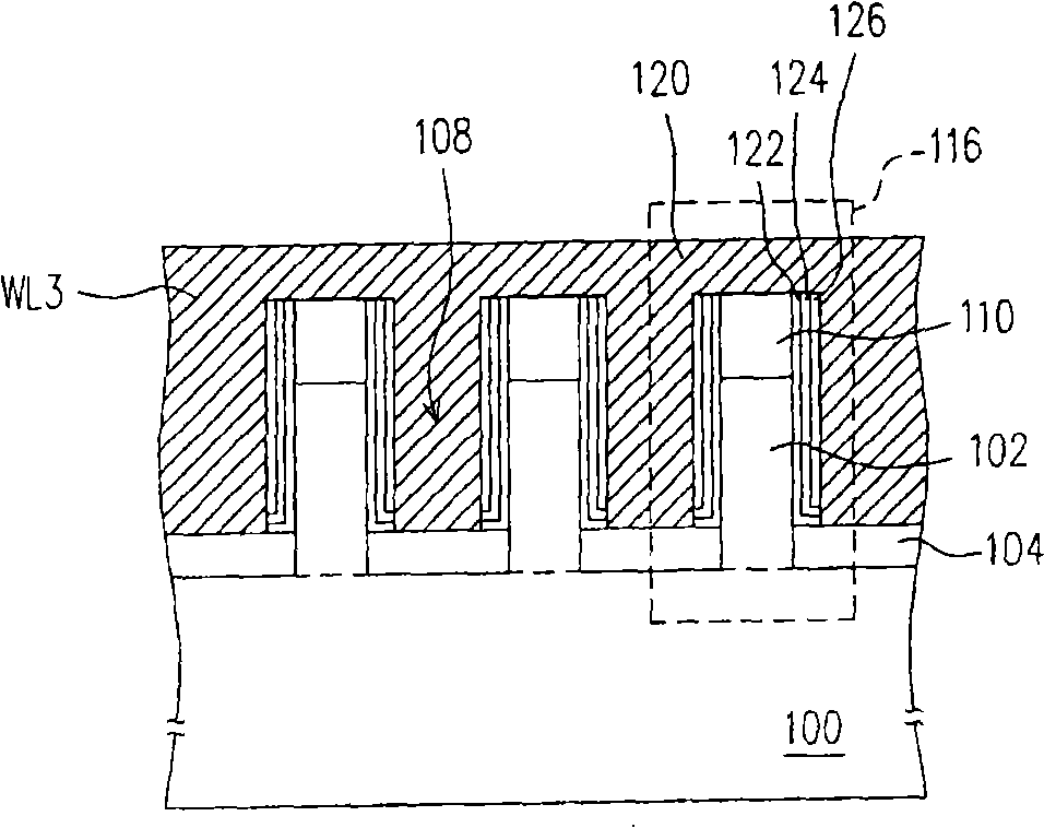
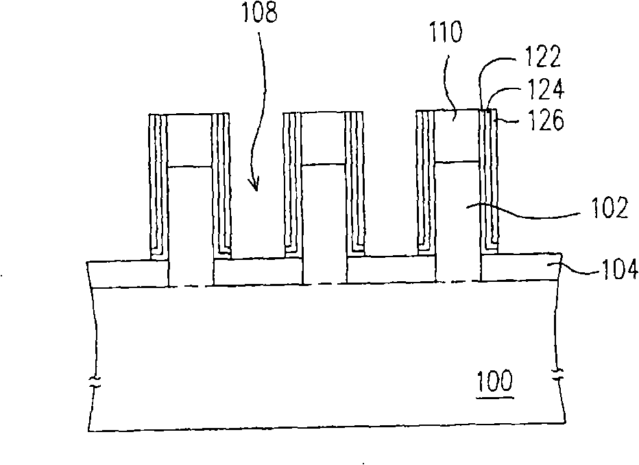
[0096] First, please refer to Figure 1A to Figure 1F , to illustrate the nonvolatile memory of the present invention. The nonvolatile memory of the present invention includes a substrate 100, multiple active layers 102, element isolation layers 104, multiple memory cell rows 106, multiple word lines WL1WL4, multiple bit lines BL1-BL3, and multiple source lines SL (only one is shown in ...


PUM


Abstract

The invention discloses a nonvolatile memory, which includes a basement, an active layer, an element isolation layer and a memory cell. The active layer is arranged on the basement and protrudes from the surface of the basement. A plurality of element isolation layers are arranged on both sides of the active layer, and the surface of the element isolation layer is lower than the surface of the active layer. The memory cell comprises a control grid, a charge storage layer, a roof cover layer and a source electrode/drain electrode region. The control grid is arranged on the basement across the active layer. The charge storage layer is arranged on the lateral wall of the active layer and is located between the control grid and the active layer. The roof cover layer is arranged on the top of the active layer and is located between the control grid and the active layer. The source electrode/drain electrode region is arranged in the active layer at the both sides of the control grid.

Description

technical field [0001] The present invention relates to a semiconductor element, and in particular to a nonvolatile memory and a manufacturing method thereof. Background technique [0002] Among all kinds of memory products, non-volatile memory, which has the advantage of being able to store, read or erase data multiple times, and the stored data will not disappear after power off, has become a personal A memory element widely used in computers and electronic equipment. [0003] A typical EEPROM uses doped polysilicon to make a floating gate and a control gate. However, when there are defects in the tunnel oxide layer under the doped polysilicon floating gate layer, it is easy to cause leakage current of the device, which affects the reliability of the device. [0004] Therefore, in the known technology, a charge trapping layer is also used to replace the polysilicon floating gate, and the material of the charge trapping layer is, for example, silicon nitride. The silicon...

Claims


Application Information

Patent Timeline
Patent Type & Authority Applications(China)
IPC IPC(8): H01L21/8247H01L21/336H01L27/115H01L29/792
Inventor 张格荥黄丘宗
Owner POWERCHIP SEMICON CORP
Why Eureka
Try Eureka