Solar cell of high efficiency and process for preparation of the same

A solar cell, conductive technology, applied in and a field

Active Publication Date: 2008-11-12
SHANGRAO JINKO SOLAR TECH DEV CO LTD
View PDF2 Cites 20 Cited by
  • Summary
  • Abstract
  • Description
  • Claims
  • Application Information

AI Technical Summary

Problems solved by technology

However, this patent relates to a technology using silicon oxynitride and silicon nitride as a dielectric material for current harvesting and thus as described below, this patent is not related to the use of silicon oxynitride and silicon nitride as a passivation layer for solar cells Significantly different from the present invention of the anti-reflection layer

Method used


Image

  • Solar cell of high efficiency and process for preparation of the same

Examples


Embodiment 1

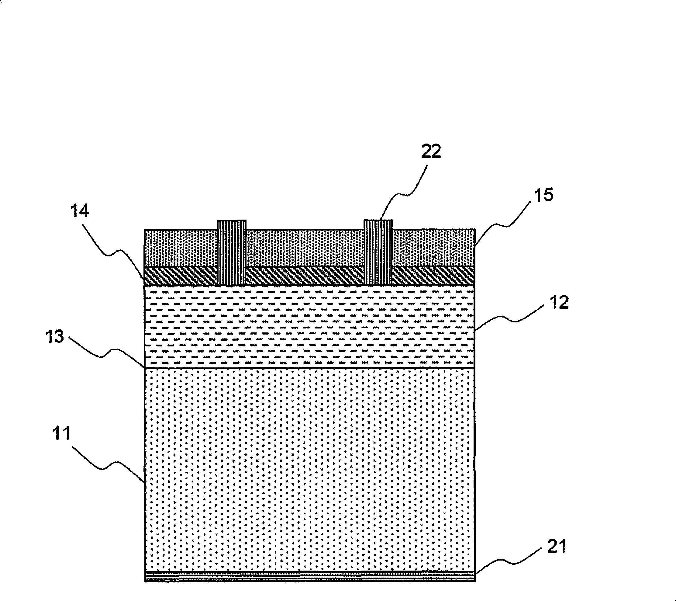
[0038] A phosphorus-doped n-type emitter layer is formed on a boron-doped p-type silicon substrate to form a p-n junction. Deposit silicon oxynitride (SiO) as a passivation layer with a thickness of 30 nm on the n-type emitter layer by PECVD x N y). Afterwards, by PECVD method, on the silicon oxynitride passivation layer, deposit the silicon nitride (SiN) with the refractive index of 1.9 as the anti-reflection layer. x ). Next, an aluminum-containing paste was screen-printed on the p-type silicon substrate and a silver-containing paste was screen-printed on the silicon nitride layer, thereby forming a pattern. The resulting structure was baked at about 800° C. for about 30 seconds to simultaneously form a rear electrode connected to the p-type silicon substrate and a front electrode connected to the n-type emitter layer, thereby preparing a solar cell.

experiment Embodiment 1

[0044] In order to measure the efficiencies of the solar cells prepared in Example 1 and Comparative Examples 1 and 2, open circuit voltage (Voc) and short circuit current (Jsc) were measured, respectively. Afterwards, based on the measured Voc and Jsc values, fill factor (FF) and solar cell efficiency were measured. The obtained results are shown in Table 1. Here, fill factor (FF) is defined as (Vmp x Jmp) / (Voc x Jsc), where Jmp and Vmp represent current density and voltage at the maximum power point. Solar cell efficiency refers to Pmax / Pin, where Pmax represents the maximum power generated by the cell and power input, and Pin is defined as the incident light intensity entering the system, that is, the light energy supplied to the system per unit time.

[0045]

[0046] Example number

[0047] As can be seen from the results in Table 1, compared with the double-reflection film structure (comparative example 1) of the silicon dioxide passivation layer and the ant...


PUM


Abstract

Disclosed herein is a high-efficiency solar cell. More specifically, provided is a solar cell comprising a first conductivity type semiconductor substrate, a second conductivity type semiconductor layer formed on the first conductivity type semiconductor substrate and having a conductivity type opposite to that of the substrate, a p-n junction at an interface therebetween, a rear electrode in contact with at least a portion of the first conductivity type semiconductor substrate, a front electrode in contact with at least a portion of the second conductivity type semiconductor layer, and a silicon oxynitride passivation layer and a silicon nitride anti-reflective layer sequentially formed on a rear surface of the first conductivity type semiconductor substrate and / or a front surface of the second conductivity type semiconductor layer; and a process for preparing the same.

Description

technical field [0001] The invention relates to a high-efficiency solar cell. More specifically, the present invention relates to a solar cell formed by sequentially forming a p-n junction with a first conductivity type semiconductor substrate and having a second conductivity type semiconductor layer having a conductivity type opposite to that of the first conductivity type semiconductor substrate. Form a silicon oxynitride passivation layer and a silicon nitride anti-reflection layer, minimize the reflectance of absorbed light through the double-reflection film structure composed of the passivation layer and the anti-reflection layer, and effectively prevent the occurrence of The carrier recombination can improve the photoelectric conversion efficiency. In addition, the present invention provides a method of preparing a solar cell capable of reducing production costs through the mass production capability of in-situ continuous formation of a double reflection film structure....

Claims


Application Information

Patent Timeline
Patent Type & Authority Applications(China)
IPC IPC(8): H01L31/042
CPCH01L31/02168Y02E10/52Y02E10/50H01L31/0216H01L31/04H01L31/06H01L31/18
Inventor 朴铉定
Owner SHANGRAO JINKO SOLAR TECH DEV CO LTD
Why Eureka
Try Eureka