Isolator silicon based three-dimensional wedge-shaped spot-size converter and method for making same

A technology of mode spot converter and wedge mode, which is applied in the field of optoelectronics, can solve the problems of low device size accuracy, high process requirements, and poor controllability, and achieve the effects of improving coupling efficiency, simple process, and strong controllability

Inactive Publication Date: 2008-11-19
SHANGHAI INST OF MICROSYSTEM & INFORMATION TECH CHINESE ACAD OF SCI
View PDF0 Cites 18 Cited by
  • Summary
  • Abstract
  • Description
  • Claims
  • Application Information

AI Technical Summary

Problems solved by technology

This method is mainly realized by deep ultraviolet exposure technology, which has high process requirements, c

Method used


Image

  • Isolator silicon based three-dimensional wedge-shaped spot-size converter and method for making same
  • Isolator silicon based three-dimensional wedge-shaped spot-size converter and method for making same
  • Isolator silicon based three-dimensional wedge-shaped spot-size converter and method for making same

Examples


Embodiment 1

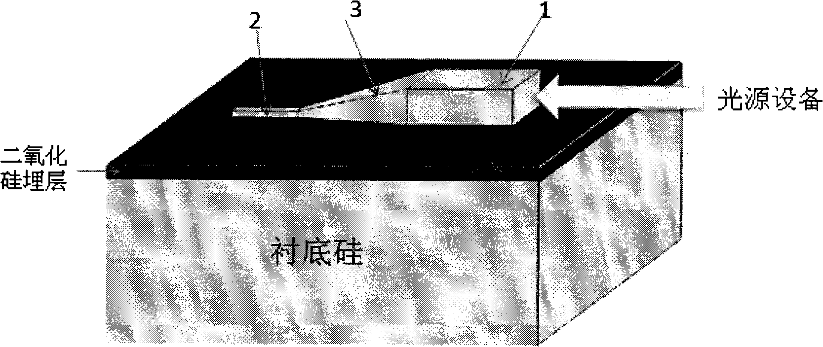
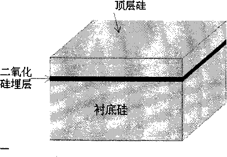
[0039] A 4-inch SOI wafer is selected, the top silicon crystal plane is (111), the thickness is 6μm, and the buried layer is SiO 2 The thickness is 1 μm, and the substrate silicon crystal plane is (100). The coupling length of the three-dimensional wedge-shaped mode-spot converter is set to 70 μm, and the input / output waveguide dimensions of the coupler are 6 μm×6 μm and 1 μm×1 μm, respectively.

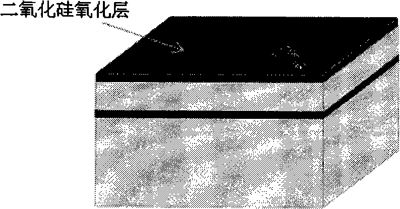
[0040] (1) Oxidation. Formed on the surface of the initial SOI material with a thickness of oxide layer.

[0041] (2) Photolithography, HF corrosion. An etching window with a size of 70 μm×100 μm is formed on the oxide layer by etching.

[0042] (3) Corrode in 40% KOH solution at 55°C for 1.5-2 hours.

[0043] (4) Clean and remove the oxide layer. A (111) slope with a thickness linearly varying from 6 μm to about 1 μm was obtained.

[0044] (5) Photolithography, etching. The output waveguide area of ​​the coupler (the area connected to the small size end of the bevel) is dry...

Embodiment 2

[0050] A 4-inch SOI wafer is selected, the top silicon crystal plane is (111), the thickness is 9 μm, and the buried layer is SiO 2 The thickness is 0.5 μm, and the substrate silicon crystal plane is (110). The coupling length of the three-dimensional wedge-shaped mode-spot converter is set to 130 μm, and the input / output waveguide dimensions of the coupler are 9 μm×9 μm and 0.5 μm×0.5 μm, respectively.

[0051] (1) Oxidation. Formed on the surface of the initial SOI material with a thickness of oxide layer.

[0052] (2) Photolithography, HF corrosion. An etching window with a size of 130 μm×130 μm is formed on the oxide layer by etching.

[0053] (3) Corrode in 40% TMAH solution at 50°C for 2-3.5 hours.

[0054] (4) Clean and remove the oxide layer. A (111) slope with a thickness linearly varying from 9 μm to about 0.5 μm was obtained.

[0055] (5) Photolithography, etching. The output waveguide area of ​​the coupler (the area connected to the small size end of the b...


PUM

PropertyMeasurementUnit
Sizeaaaaaaaaaa
Thicknessaaaaaaaaaa

Abstract

The invention relates to an SOI-based (silicon on insulator) three-dimensional wedge-shaped spot-size converter based on micromachining as well as a making method thereof, which are used for realizing the high efficiency coupling between light source equipment such as optical fibers and small-sized optoelectronic devices such as silica-based wave guide. The spot-size converter is made by utilizing selectivity corrosion characteristics of different crystal faces of a silicon wafer and adopting the bulk silicon micro-machining technique, and belongs to the microelectronics and solid electronics fields. The converter is made by adopting SOI materials and utilizing micromachining processes such as photolithography, anisotropy corrosion and dry etching for processing, so as to obtain the three-dimensional wedge-shaped spot-size converter structure having linear variation in both the vertical and horizontal directions, thereby effectively improving the coupling efficiency of optical and optoelectronic devices such as general optical fibers and small-sized plane wave guide. The making method of the invention has the advantages of simple processes, good compatibility, and strong controllability and practicability.

Description

technical field [0001] The invention belongs to the field of optoelectronic technology, and in particular relates to a SOI (Silicon-On-Insulator Silicon on Insulator)-based three-dimensional wedge-shaped spot converter based on micromachining, specifically a selection using different crystal planes of silicon wafers Corrosion characteristics, using bulk silicon micromachining technology to realize the fabrication method of SOI-based three-dimensional wedge-shaped spot converter. Background technique [0002] Since the 1960s, optoelectronic integration has made great progress. The mainstream trend of integrated circuit development is the miniaturization of integrated systems. Among the many waveguide materials used in the communication band, the unique sandwich structure of SOI materials has unique advantages in the preparation of optoelectronic devices. The refractive indices of silicon and silicon dioxide materials are 3.45 and 1.4, respectively, and the high-contrast refr...

Claims


Application Information

Patent Timeline
IPC IPC(8): G02B6/26G03F7/00
Inventor 方娜杨志峰武爱民陈静王曦
Owner SHANGHAI INST OF MICROSYSTEM & INFORMATION TECH CHINESE ACAD OF SCI
Why Eureka
Try Eureka