Ion injection method of semiconductor device

An ion implantation and semiconductor technology, which is applied in semiconductor/solid-state device manufacturing, electrical components, circuits, etc., can solve the problems of semiconductor device performance attenuation and lower yield, and achieve the effect of reducing attenuation and improving yield

Inactive Publication Date: 2008-11-19
SEMICON MFG INT (SHANGHAI) CORP
View PDF0 Cites 9 Cited by
  • Summary
  • Abstract
  • Description
  • Claims
  • Application Information

AI Technical Summary

Problems solved by technology

Since the structure of the undoped polysilicon layer is a typical columnar grain, in the process of decelerating ion implantation to the polysilicon layer, because the ion implantation concentration is generally high, the implanted ions are easy to penetrate through the grain boundary edge of the polysilicon layer. On the silicon substrate of the semiconductor, which leads to the attenuation of the performance of the semiconductor device and reduces the yield

Method used


Image

  • Ion injection method of semiconductor device

Examples


Embodiment Construction

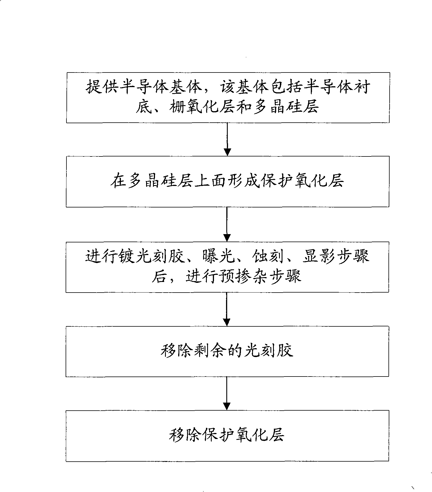
[0014] Combine below figure 1 The ion implantation method disclosed in the present invention is further described in detail.

[0015] The ion implantation method of the present invention comprises the following steps:

[0016] A semiconductor base is provided, which includes a semiconductor silicon substrate, a gate oxide layer deposited on the substrate, and a polysilicon layer deposited on the gate oxide layer as a gate of a semiconductor device;

[0017] A thin protective oxide layer is formed on the polysilicon layer. The protective oxide layer can be formed in a high-temperature furnace or in a rapid thermal oxidation system (rapid thermal oxidation, RTO), wherein the thickness of the protective oxide layer is The range is 20-100 Angstroms;

[0018] Plating a photoresist on the protective oxide layer can be based on the photoresist characteristics, plating a positive photoresist or a negative photoresist, and then performing exposure, etching, and developing steps at a ...


PUM


Abstract

The invention discloses an ion injection method, relating to semiconductor manufacturing technical field. The ion injection method includes the following steps: a semiconductor basal body is provided, comprising a semiconductor substrate, a gate oxide layer deposited at the semiconductor substrate and a polycrystalline silicon layer arranged on the gate oxide layer; a protecting oxide layer is built on the polycrystalline silicon layer; the protecting oxide layer is plated with light-sensitive lacquer and then is exposed in light, etched and developed; pre-doping process is started and the injected ions penetrate the protecting oxide layer and reach the polycrystalline silicon layer; the light-sensitive lacquer is removed and then the protecting oxide layer is removed. Compared with prior art, the ion injection method of the invention avoids or at least reduces the injected ions that penetrate into the semiconductor substrate by adding a protecting oxide layer on the polycrystalline silicon layer, thus reducing the attenuation of the performance of the semiconductor.

Description

technical field [0001] The invention relates to the manufacturing technology in the field of semiconductors, in particular to an ion implantation method capable of reducing performance attenuation of semiconductor devices. Background technique [0002] Semiconductor devices generally include a semiconductor silicon substrate, a gate oxide layer (usually silicon dioxide, or silicon nitride, etc.) on the substrate, and a polysilicon layer deposited on the gate oxide layer, wherein the polysilicon layer is the semiconductor device. grid. With the development of semiconductor technology, the operating speed of semiconductor devices is getting faster and faster, the integration of chip circuits is getting higher and higher, and the power consumption is getting lower and lower, so that the characteristic size of the polysilicon gate of the semiconductor device (critical dimension, CD), the thickness of the gate oxide layer and other parameters gradually become smaller, so that it...

Claims


Application Information

Patent Timeline
Patent Type & Authority Applications(China)
IPC IPC(8): H01L21/266
Inventor 何永根戴树刚
Owner SEMICON MFG INT (SHANGHAI) CORP
Why Eureka
Try Eureka