
Silicon with three-dimensional depression structure and method for preparing same

A three-dimensional hollow and hollow technology, applied in chemical instruments and methods, single crystal growth, single crystal growth, etc., can solve the problems of unreported preparation methods, and achieve the effects of easy control of preparation parameters, simple preparation steps, and cheap raw materials

Inactive Publication Date: 2011-01-26
PEKING UNIV
View PDF0 Cites 0 Cited by
  • Summary
  • Abstract
  • Description
  • Claims
  • Application Information

AI Technical Summary

Problems solved by technology

[0006] At present, the preparation method of this kind of silicon with a roof-shaped three-dimensional hollow structure has not been reported.

Method used


Image

  • Silicon with three-dimensional depression structure and method for preparing same
  • Silicon with three-dimensional depression structure and method for preparing same
  • Silicon with three-dimensional depression structure and method for preparing same

Examples


Embodiment 1

[0027] In this embodiment, the reaction raw materials used are 10mm×10mm silicon wafer (111 sides), chemically pure metal zinc powder.

[0028] Firstly, the silicon wafer is cleaned by Pilar method to remove the oxide layer on the surface and impurities adsorbed on the surface. The size of the silicon wafer is generally cut into 10mm×10mm.

[0029] First put 3-4 pieces of silicon wafers face up, arrange them in sequence, place them in the quartz boat, and cover the silicon wafers with a layer of metal zinc powder, each with a mass of 0.2-0.3g. The quartz boat is placed in the center of the tube-type heating furnace. In addition, the quartz boat that is also equipped with 3-4 pieces of silicon wafers but not covered with zinc powder is placed in the lower tuyere 15cm away from the center of the tube-type heating up furnace.

[0030] After the sample is loaded into the tube-type heating furnace and sealed completely, the mechanical pump is turned on to pump air, so that the pre...

Embodiment 2

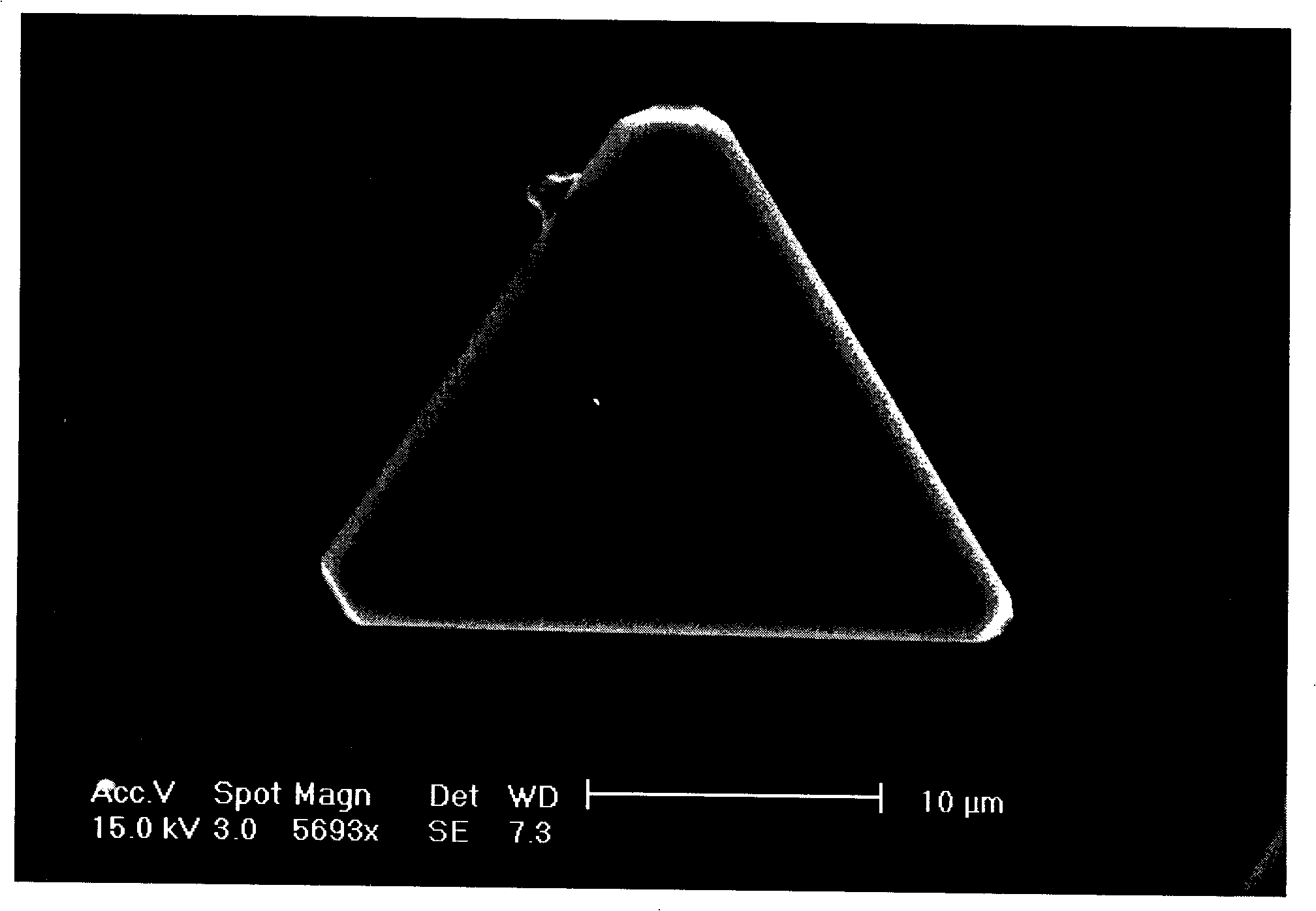
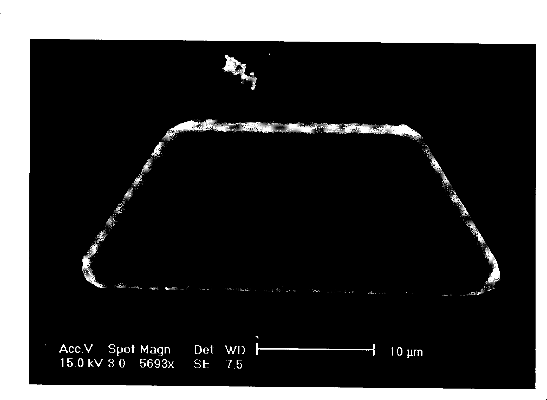
[0035] In this embodiment, the highest temperature is set above 1300°C, and other conditions are the same as in Embodiment 1. The pyramid or roof structure obtained on the silicon chip is not complete, and many gaps appear, such as Figure 5 shown.

Embodiment 3

[0037] In this embodiment, the silicon wafer is not covered or thermally evaporated and deposited with zinc powder, and other conditions are the same as in Embodiment 1, only the silicon wafer is heated, and finally no three-dimensional structure of silicon can be obtained.

[0038] It can be seen from the above three examples that the silicon with a three-dimensional hollow structure is obtained by reacting the metal zinc powder and the silicon sheet at high temperature. Other parameters, such as maximum temperature, pressure and holding time, and whether oxygen is introduced or not will also affect the growth of the three-dimensional structure of silicon. Wherein, those skilled in the art can understand that the amount of zinc powder used, the size of the silicon wafer, and the ventilation rate of oxygen are determined according to the heating equipment, and are not limited to the scope given by the embodiments of the present invention.


PUM

PropertyMeasurementUnit
heightaaaaaaaaaa
lengthaaaaaaaaaa

Abstract

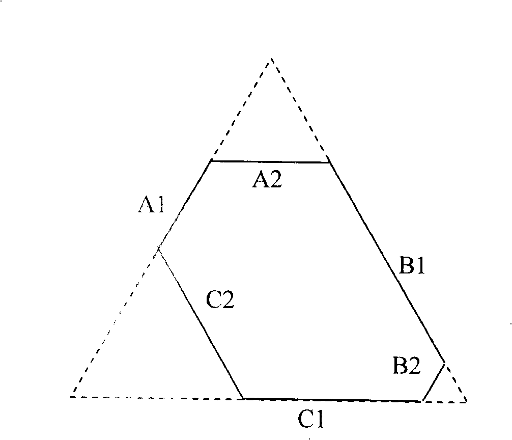
The invention discloses silicon with a three-dimensional sunken structure and a preparing method thereof, which belongs to the field of semiconductor material and preparation thereof. The three-dimensional sunken structure of the silicon with the three-dimensional sunken structure of the invention is in the shape of a right prism, wherein, the undersurface is a polygon which sequentially consistsof side A1, A2, B1, B2, C1 and C2, wherein, side A1 is parallel to A2; side B1 is parallel to B2; side C1 is parallel to C2; triangles formed by three intersections obtained by intersecting of two ofstraight lines where A1, B1 and C1 or A2, B2 and C2 lie are regular triangles. The inside part of the three-dimensional structure is hollow. Meanwhile, the invention provides a method for preparing the silicon with the three-dimensional sunken structure by a vapor deposition method, wherein, the method is that the silicon with the three-dimensional solid structure grows by the eutectic melting ofthe sediment of zinc and silicon on the surface of silicon. Compared with the prior art, the invention has the advantages that raw material of the preparation is very cheap; the preparing procedures are simple and easy to be repeated; the preparation parameter is easy to control; the crystallization of a generated product is good; a regular three-dimensional solid structure is provided.

Description

technical field [0001] The invention relates to silicon with a three-dimensional hollow structure and a preparation method thereof, belonging to the field of semiconductor materials and preparation thereof. Background technique [0002] Silicon is one of the most important materials in semiconductor technology, and it is of great significance to grow nano or micro structures on silicon. [0003] Nanomaterials with special structures and their novel properties have become a research hotspot. Many physical phenomena of these materials have been predicted and confirmed. The growth of three-dimensional structures on silicon surfaces is also the focus of recent research. This three-dimensional structure obtained by self-assembly growth has important application prospects in fields such as optoelectronic devices. [0004] The three-dimensional structure involved in the present invention has a straight prism shape, and its outer surface can be used as a substrate for growing oth...

Claims


Application Information

Patent Timeline
Patent Type & Authority Patents(China)
IPC IPC(8): C30B29/06C30B29/60
Inventor 奚中和吴越张耿民崔宏宇郭等柱
Owner PEKING UNIV
Learn More