Low-cost high-efficient time division multiplex charge pump circuit

A technology of time-sharing multiplexing and charge pump, which can be applied in the direction of conversion equipment without intermediate conversion to AC, which can solve the problems of limited circuit efficiency, large chip area, and reduced power supply voltage of process feature size.

Inactive Publication Date: 2008-12-31
天利半导体(深圳)有限公司
View PDF0 Cites 12 Cited by
  • Summary
  • Abstract
  • Description
  • Claims
  • Application Information

AI Technical Summary

Problems solved by technology

But this will undoubtedly occupy a large chip area, so there is a literature that proposes a charge pump circuit based on coupling capacitor sharing and is applied to the field of flash memory circuit design; figure 2 It is the circuit diagram of this charge pump. CK1 and CK2 are two-phase non-overlapping clocks. The positive charge pump and the negative charge pump share a set of capacitors through a set of coupling switches controlled by VCP and VCN; where the PMOS and NMOS in the coupling switch The substrate terminals of the system are respectively connected to the most positive voltage VPP and the most negative voltage VPN of the system, which seriously restricts the efficiency of the circuit and increases the internal friction of the circuit; in addition, the circuit uses a PMOS transmission tube to transmit low-level , Using NMOS transmission tube to transmit high level, there is a loss of threshold voltage, so only positive high voltage of (N+1)*(VCI-Vt) and negative high voltage of -N*(Vt-VCI) can be generated, of which N is the number of stages of the charge pump, Vt is the threshold of the transmission tube
In this way, for a given voltage, more stages, that is, more area, will be required to realize the circuit design; and this problem will become more and more serious with the continuous reduction of process feature size and the continuous reduction of system power supply voltage.

Method used


Image

  • Low-cost high-efficient time division multiplex charge pump circuit
  • Low-cost high-efficient time division multiplex charge pump circuit
  • Low-cost high-efficient time division multiplex charge pump circuit

Examples


Embodiment Construction

[0022] The specific embodiment of the present invention will be described with reference to the accompanying drawings.

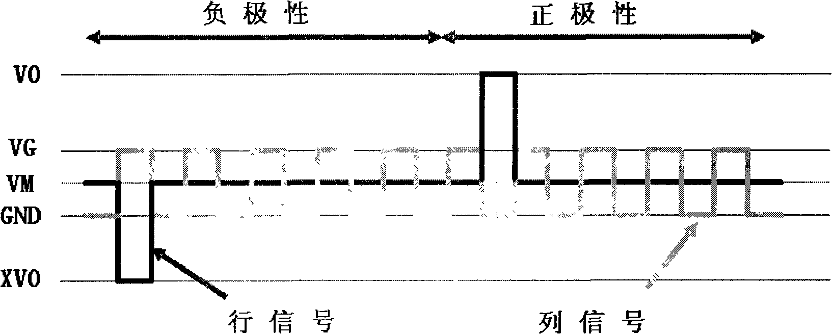
[0023] figure 1 It is the driving waveform diagram of the LCD driving circuit based on the HiFas scanning method.

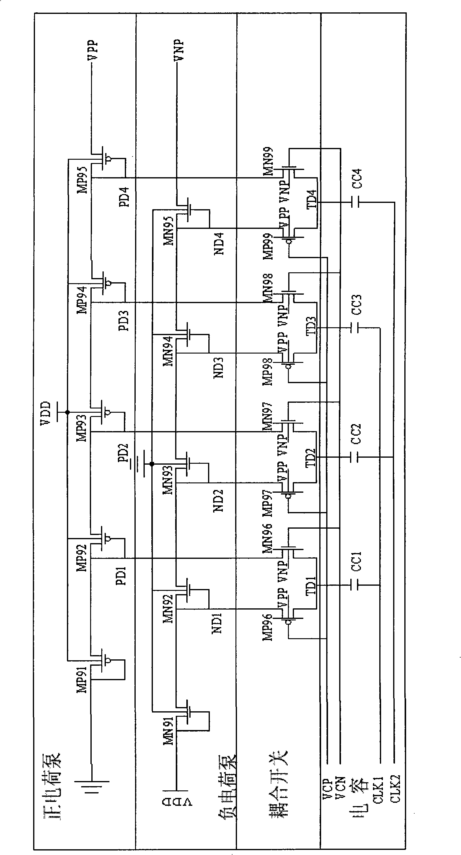
[0024] figure 2 It is a circuit diagram of a charge pump based on coupling capacitor sharing.

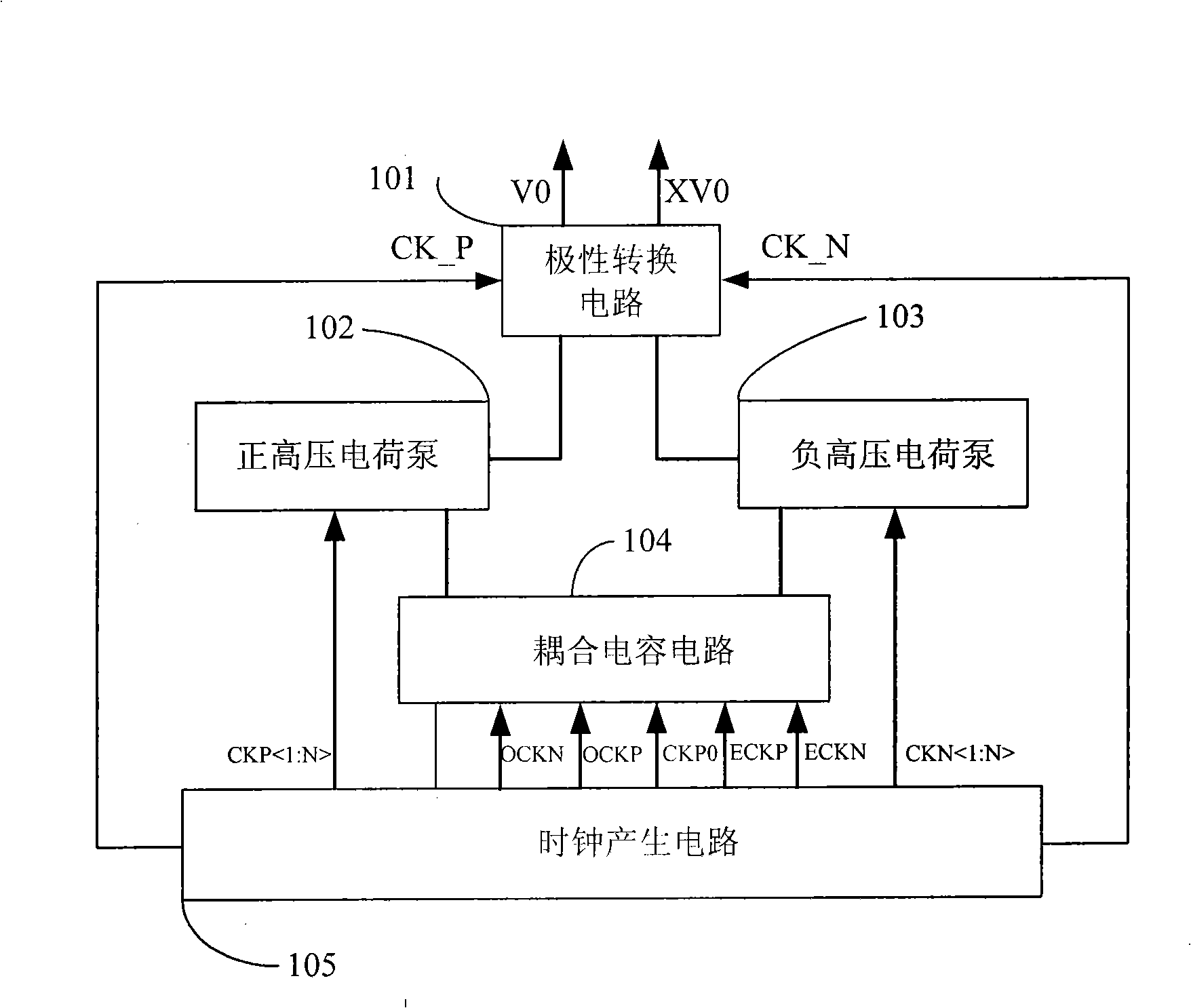
[0025] Such as image 3 , in order to realize the time-division generation of positive high voltage and negative high voltage, in the positive polarity, the clock generation circuit 105 turns off the negative high voltage charge pump 103, and the positive high voltage charge pump 102, the coupling capacitor circuit 104 and the polarity conversion circuit 101 are in the clock generation circuit Under the control of 105, positive high voltage V0 is generated; in negative polarity, clock generation circuit 105 shuts off positive high voltage charge pump 102, and negative high voltage charge pump 103, coupling capacitor circuit 104 and polarity conve...


PUM


Abstract

The invention relates to a time-sharing multiplex charge pump circuit with low cost and high efficiency, belonging to the fields of the analog integrated circuit design and LCD drive circuit design, and particularly relates to the LCD drive circuit design based on an HiFas (High Frequency Amplitude Selection) scanning way. The circuit is characterized in that the system adopts a time-sharing multiplex technology for reducing the design requirements of a technological pressure-resisting value; a space overlapping technology is adopted in the design of a coupling capacitor, therefore, the area of a chip is more rationally utilized. In the design of a polarity conversion circuit, an external capacitor can be saved by flexibly switching the voltage on a capacitor polar plate. In the design of a positive high-pressure charge pump and a negative high-pressure charge pump, a zero bulk-biased technology and a charge sharing technology are used, thus enhancing the charge transferring efficiency and reducing the internal friction of the circuit. By utilizing the technologies, the circuit can substantially reduce design cost and enhance circuit efficiency.

Description

technical field [0001] A low-cost, high-efficiency, time-division multiplexing charge pump circuit belongs to the fields of analog integrated circuit design and LCD drive circuit design, and particularly relates to the design of an LCD drive circuit based on HiFas scanning mode. Background technique [0002] In many integrated circuit systems, it is necessary to generate a positive high voltage or a negative high voltage higher than the power supply voltage VCI on-chip. figure 1 It is the driving waveform of the LCD driving circuit based on the HiFas scanning method. The column voltages VG and GND, the positive high voltage V0 and the negative high voltage XV0 are all symmetrical about the row voltage VM. In addition, the system needs to generate a positive high voltage V0 as the row selection when it is positive. Signal; in negative polarity, a negative high voltage XV0 needs to be generated as a row selection signal. [0003] Traditionally, two separate charge-pump circui...

Claims


Application Information

Patent Timeline
Patent Type & Authority Applications(China)
IPC IPC(8): H02M3/07
Inventor 林昕林丰成陈博韩双
Owner 天利半导体(深圳)有限公司
Why Eureka
Try Eureka