Method of manufacturing semiconductor device
A manufacturing method and semiconductor technology, applied in semiconductor/solid-state device manufacturing, electrical components, circuits, etc., can solve problems such as increased resistance and inability of field-effect transistors to work at high speeds, and achieve the effect of improving reliability and performance
- Summary
- Abstract
- Description
- Claims
- Application Information
AI Technical Summary
Problems solved by technology
Method used
Image
Examples
Embodiment approach 1
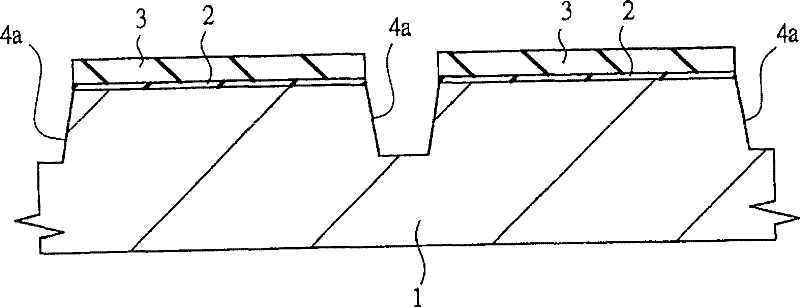
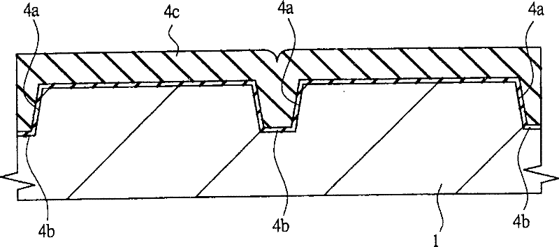
[0152] Next, the semiconductor device manufacturing process of this embodiment will be described with reference to the drawings. Figure 1 to Figure 8 It is a sectional view of main parts in the manufacturing process of a semiconductor device which is one embodiment of the present invention, for example, a semiconductor device having a CMISFET (Complementary Metal Insulator Semiconductor Field Effect Transistor).
[0153] First, if figure 1 As shown, a p-type semiconductor substrate (semiconductor wafer) 1 made of single crystal silicon or the like having a resistivity of, for example, about 1 to 10 Ωcm is prepared. Then, the semiconductor substrate 1 is thermally oxidized to form an insulating film 2 with a thickness of about 11 nm, for example, on the surface thereof, and then deposited on the upper layer of the insulating film with a thickness of about 90 nm by CVD (Chemical Vapor Deposition) or the like. The insulating film 3. The insulating film 2 is made of silicon oxi...
Embodiment approach 2
[0322] Figure 31 is a manufacturing process flowchart showing a part of the semiconductor device manufacturing process of this embodiment, and corresponds to the above-mentioned first embodiment. Figure 9 . Figure 31 means to get the above Figure 7 After the structure of the gate electrode 8a, 8b, n + type semiconductor region 9b and p + The manufacturing process flow of the step of forming a metal silicide layer (metal-semiconductor reaction layer) on the surface of the type semiconductor region 10b. Figure 32 ~ Figure 35 It is a sectional view of main parts in the manufacturing process of the semiconductor device of this embodiment.
[0323] In the manufacturing process of the semiconductor device of this embodiment, the steps up to the removal of the isolation film 13 and the unreacted metal film 12 by wet cleaning in the above-mentioned step S4 are the same as the above-mentioned embodiment 1, so the description is omitted here, and the above-mentioned step S4 Th...
Embodiment approach 3
[0339] The inventors of the above Figure 18 ~ Figure 21 After further research on the process of the comparative example, it was found that compared with the n-channel MISFET, the source and drain of the p-channel MISFET are prone to increase in junction leakage current and uneven junction leakage due to the formation of the nickel silicide layer 141b. (variation of junction leakage current for each transistor).
[0340] In order to reduce the above-mentioned junction leakage current, it is effective to reduce the thickness of the Ni film 112 deposited on the semiconductor substrate 1, thereby reducing the thickness of the nickel silicide layer 141b. However, the nickel silicide layer 141b is provided for low resistance. Therefore, if the thickness of the nickel silicide layer 141b of both the n-channel type MISFET and the p-channel type MISFET is reduced, even the n-channel type MISFET that is less likely to affect the junction leakage current will cause the nickel silicide...
PUM
 Abstract
Description
Claims
Application Information


