

Phase-changing storage device and manufacture method thereof
A technology of phase change memory and manufacturing method, applied in static memory, digital memory information, information storage and other directions, can solve problems such as insufficient filling of gaps and insufficient filling
- Summary
- Abstract
- Description
- Claims
- Application Information
AI Technical Summary
Problems solved by technology
Method used
Image

Examples
no. 1 example
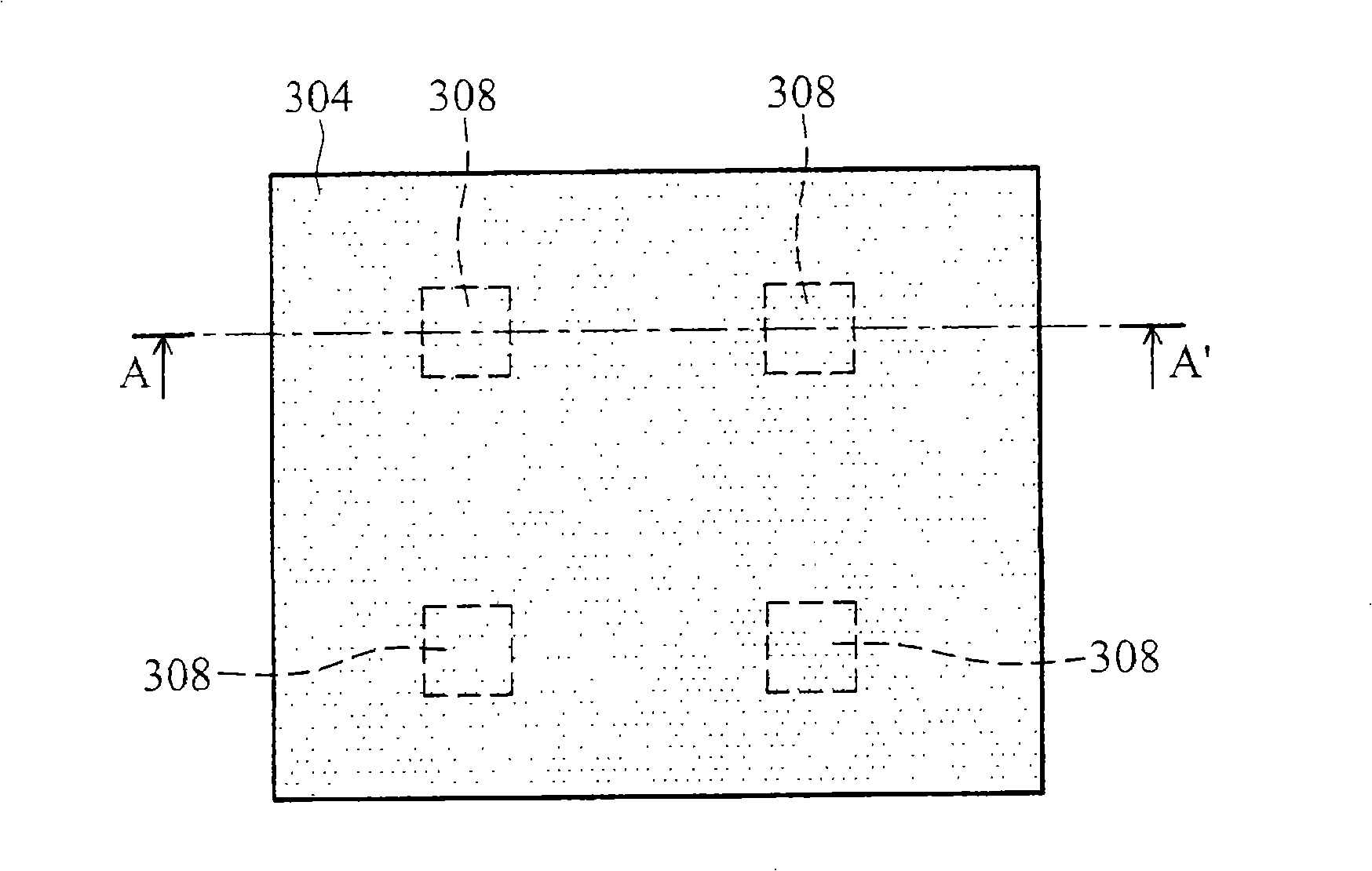
[0049] Please refer to Figure 2a , which shows a top view of the manufacturing process of the phase change memory device according to the first embodiment of the present invention; please refer to Figure 2b , which shows a cross-sectional view of the manufacturing process of the phase change memory device according to the first embodiment of the present invention. A substrate 300 is provided, and the substrate 300 is a silicon substrate. In other embodiments, silicon germanium (SiGe), bulk semiconductor (bulk semiconductor), strained semiconductor (strained semiconductor), compound semiconductor (compound semiconductor), silicon on insulator (SOI) or Other common semiconductor substrates. The substrate 300 may also be a substrate including electronic components such as transistors, diodes, bipolar junction transistors (BJTs), resistors, capacitors, and inductors. Then, for example, physical vapor deposition (physical vapor deposition, PVD), sputtering (sputtering), low pr...
no. 2 example
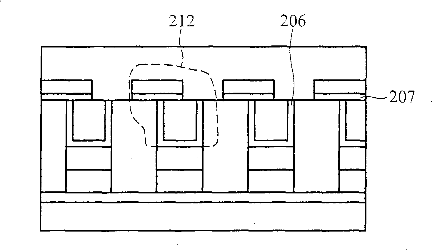
[0069] Please refer to Figure 16a and 16b , which shows the formation of the cup-shaped opening 318 in the second embodiment of the present invention, wherein the element and Figure 2a , 2b For the same parts shown in ~6a and 6b, reference may be made to the previous relevant descriptions, and repeated descriptions are not repeated here. use Figure 6a , 6b The hard mask layer 310 a and the photoresist layer 316 are shown as an etching hard mask, and an anisotropic etching step is performed to remove part of the dielectric layer 304 until the switching element 308 is exposed. Next, the photoresist layer 316 may be removed by a photoresist stripping (PR stripping) process such as photoresist asher. Then, the hard mask layer 310 a can be removed by dry etching or wet etching to form a cup-shaped opening 318 , the bottom of which is overlay aligned above the switching element 308 . In the embodiment of the present invention, the etching selectivity ratio between the hard ...
PUM
| Property | Measurement | Unit |
|---|---|---|
| Thickness | aaaaa | aaaaa |
| Thickness | aaaaa | aaaaa |
| Thickness | aaaaa | aaaaa |
Abstract
Description
Claims
Application Information