
Double-face nanometer band electrode array integration sensor capable of being cut and method for manufacturing same

An integrated sensor and electrode array technology, applied in the field of chemical and biological sample detection, can solve complex problems, achieve the effect of less interference, fast measurement, and less sample solution

Inactive Publication Date: 2009-02-04
ZHEJIANG UNIV
View PDF0 Cites 11 Cited by
  • Summary
  • Abstract
  • Description
  • Claims
  • Application Information

AI Technical Summary

Problems solved by technology

The microelectrode array has good stability and repeatability, but it generally needs to be used with a reference electrode to form an electrode test system, which is relatively complicated.

Method used


Image

  • Double-face nanometer band electrode array integration sensor capable of being cut and method for manufacturing same
  • Double-face nanometer band electrode array integration sensor capable of being cut and method for manufacturing same
  • Double-face nanometer band electrode array integration sensor capable of being cut and method for manufacturing same

Examples


Embodiment Construction

[0026] The present invention will be further described below in conjunction with drawings and embodiments.

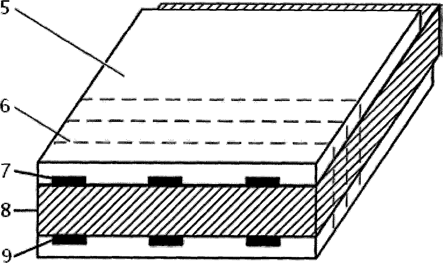
[0027] Such as figure 2 , image 3 As shown, the present invention includes a substrate, an electrode, an insulating layer, and a bonding pad. Choose silicon wafer or glass as Si / SiO 2 Substrate 8, using MEMS technology to deposit two different electrode materials on the front and back planes of the substrate to form Au working electrode 7 and Pt reference electrode 9 respectively, using photolithography technology to form a comb-shaped Au working electrode with upper and lower symmetry 7 and Pt reference electrode 9 arrays, with Si deposited on both sides of the comb-shaped working electrode and reference electrode by PECVD method 3 N 4 The insulating layer 5 is exposed to the pad 2 by photolithography, and a plurality of cutting lines 6 perpendicular to the electrode direction are engraved on both insulating layers.

[0028] The thicknesses of the Au working ele...


PUM

PropertyMeasurementUnit
thicknessaaaaaaaaaa
thicknessaaaaaaaaaa
widthaaaaaaaaaa

Abstract

The present invention discloses an electrode array integrated sensor which can cut two-sided nanobelts, and a preparation method thereof. Silicon or glass is selected as a base; the MEMS technology is adopted to deposit two different electrode materials onto the positive plane and the negative plane of the base; the lithography is used for forming a comb-shaped working electrode array and a reference electrode array, which are vertically symmetrical; the PECVD method is used for depositing a silicon nitride insulating layer respectively on two sides; the lithography extends out of the pad; the insulating layers on the two sides are provided with a plurality of cutting lines which are etched vertical to the electrodes. The sensor is used for regularly cutting and polishing, and can be repeatedly used so as to prolong the service life of the device and to enhance and maintain the consistency and stability of the electrodes. The sensor is fixed in the Teflon cavity, and adopts the differential pulse anodic stripping voltammetry to collect the impedance of the tested solution and complete the oxidation-reduction of current signals. The integrated sensor can be used for direct quantitative detection of the concentration of anions and cations in the solution in such fields as rivers and lakes, biomedicine, industrial wastewater and waste gas, and so on, and can be used for qualitative detection of biological molecules after completing the surface modification.

Description

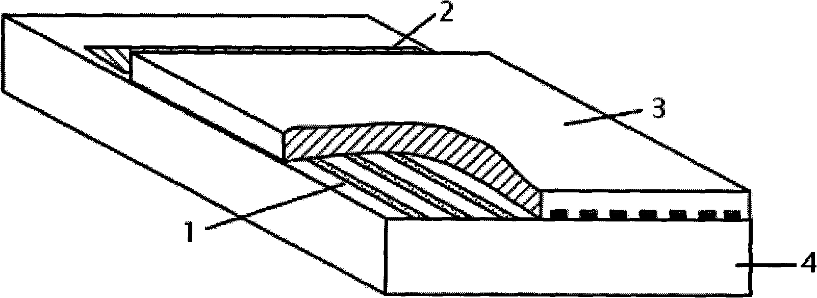
technical field [0001] The invention relates to a chemical and biological sample detection technology, in particular to a tailorable double-sided nanobelt electrode array integrated sensor. Background technique [0002] Biological and chemical substances can have beneficial effects on the human body, as well as harmful or even fatal effects. Therefore, the qualitative and quantitative detection of chemical and biological samples is of great significance in environmental, food, drug and clinical testing. The current detection methods mainly include atomic absorption spectrophotometry and mass spectrometry, etc., but the equipment used in these methods is huge and expensive, requires complex pretreatment, long measurement period and skilled operators, which brings great problems in practical applications. Many inconveniences. [0003] The structure of the existing ultramicro electrode array in the world is as follows: figure 1 As shown, it includes four parts: substrate 4 , ...

Claims


Application Information

Patent Timeline
Patent Type & Authority Applications(China)
IPC IPC(8): G01N27/00G01N33/48B81C1/00
Inventor 王平李毅付静蔡巍
Owner ZHEJIANG UNIV
Learn More