Ohm contact of gallium nitride base device and preparation method thereof

A gallium nitride-based, ohmic contact technology, applied in the direction of semiconductor devices, laser components, lasers, etc., can solve the problem that metal interdiffusion cannot be completely blocked, achieve good surface morphology, improve comprehensive performance, and high reliability Effect

Inactive Publication Date: 2009-02-18
PEKING UNIV
View PDF0 Cites 13 Cited by
  • Summary
  • Abstract
  • Description
  • Claims
  • Application Information

AI Technical Summary

Problems solved by technology

However, in the actual results, it was found that the role of Al in the ohmic contact of the above-mentioned Ti / Al / Ni / Au system is not only as mentioned above, but its role needs further research; and Ni, as a barrier metal, cannot completely To block the interdiffusion between metals, the specific role of these metals needs to be further studied

Method used


Image

  • Ohm contact of gallium nitride base device and preparation method thereof
  • Ohm contact of gallium nitride base device and preparation method thereof
  • Ohm contact of gallium nitride base device and preparation method thereof

Examples


Embodiment Construction

[0029] Below in conjunction with accompanying drawing and specific embodiment the present invention is described in further detail:

[0030] Taking AlGaN / GaN HFET devices as an example, the specific technical solutions are as follows:

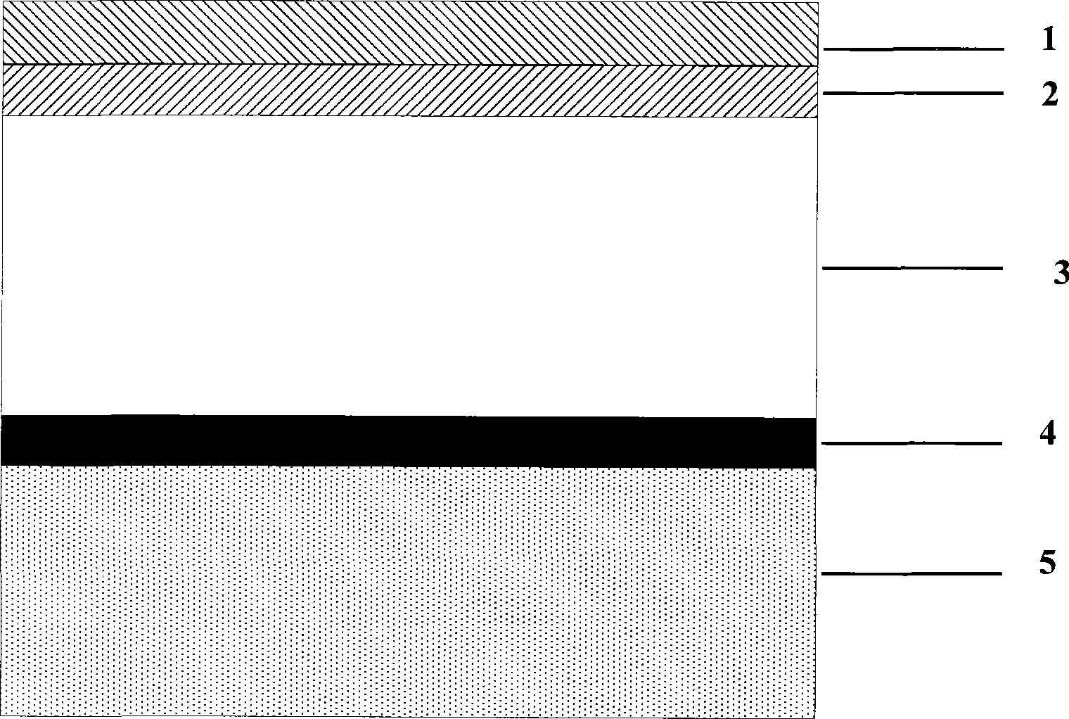
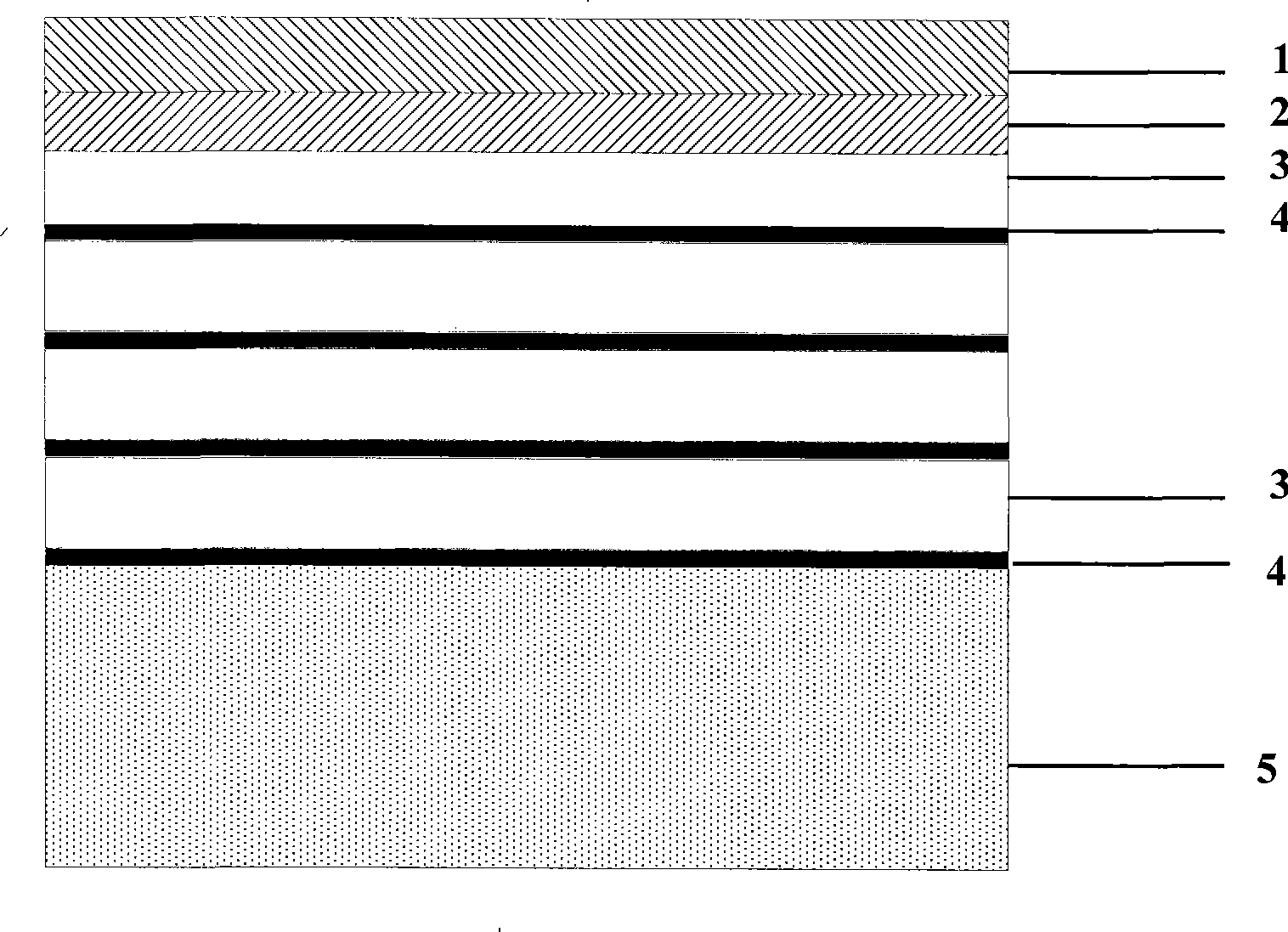
[0031] (1) Ohmic metal structure layout of photolithographic devices;

[0032] (2) Deposition of the metal layer structure, using magnetron sputtering to deposit Ti 5nm, Al 30nm, Ti 5nm, Al 30nm, Ti 5nm, Al 30nm, Ti 5nm, Al 30nm, Ni 50nm, Au 200nm.

[0033] (3) Peeling off: Ultrasonic the device sample on which the metal has been deposited in acetone to form an ohmic pattern.

[0034] (4) Rapid thermal annealing: Clean the device sample and put it into the rapid annealing furnace. Two annealing schemes are adopted: the temperature range of the first annealing is 800-900°C, and the time is 30S; the temperature range of the second annealing is 400~600℃, the time is 120S.

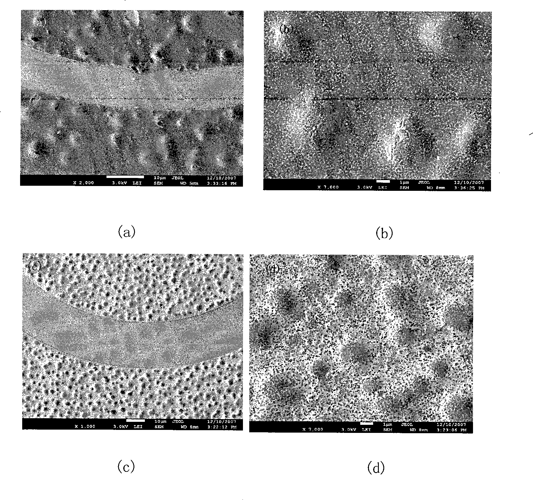
[0035] The resistivity comparison between the ohmic contact of this emb...


PUM

PropertyMeasurementUnit
thicknessaaaaaaaaaa
thicknessaaaaaaaaaa

Abstract

The invention discloses an ohmic contact of a GaN-based apparatus and a manufacturing method thereof, belonging to the technical field of semiconductors. The ohmic contact of the GaN-based apparatus is composed of a titanium metal layer, an aluminum metal layer, a barrier metal layer and a gold metal layer; the titanium metal layer is contacted with the ohmic contact of the GaN-based apparatus, the aluminum metal layer is covered on the titanium metal layer, the barrier metal layer and the gold metal layer are covered on the titanium metal layer and the aluminum metal layer in sequence, wherein, the titanium metal layer and the aluminum metal layer are overlapped in two to ten periods. Compared with the prior ohmic contact structure, the invention balances low ohmic contact ratio based on the ohmic contact of a multilayer Ti / Al structure, has good surface appearance and high reliability, can improve the combination property of the ohmic contact, and has an important meaning for realizing the GaN-based apparatus with high performance and high reliability.

Description

technical field [0001] The invention relates to a gallium nitride-based device in the field of semiconductor technology, in particular to an ohmic contact of a gallium nitride-based device and a preparation method thereof. Background technique [0002] Devices based on AlGaN / GaN materials are collectively referred to as gallium nitride-based devices, such as AlGaN / GaN heterojunction field effect transistors (heterostructure field effect transistors, HFET), heterojunction bipolar transistors (heterostructure bipolar transistor, HBT), etc. . Gallium nitride-based devices have the advantages of high operating temperature, strong breakdown field, high cut-off frequency, and high power density. [0003] Unlike traditional Si devices and GaN systems, gallium nitride-based devices cannot form ohmic contacts by heavily doping semiconductor materials. The specific process is: first, magnetron sputtering or electron beam evaporation deposition on the surface of the semiconductor requ...

Claims


Application Information

Patent Timeline
Patent Type & Authority Applications(China)
IPC IPC(8): H01L29/41H01L29/45H01L29/772H01L29/737H01L33/00H01L31/0224H01L31/18H01L21/28H01S5/00H01L33/38
CPCY02P70/50
Inventor 董志华王金延郝一龙文正王阳元
Owner PEKING UNIV
Why Eureka
Try Eureka