Thin-film diode, double scanning diode array substrate and LCD board

A technology of thin film diodes and diode arrays, applied in optics, instruments, electrical components, etc., can solve the problems of deterioration of electrical characteristics, current breakdown, and film damage of thin film diodes 132

Inactive Publication Date: 2009-03-11
AU OPTRONICS CORP
View PDF0 Cites 4 Cited by
  • Summary
  • Abstract
  • Description
  • Claims
  • Application Information

AI Technical Summary

Problems solved by technology

[0008] However, since the non-linear resistance material layer 132b is made of a silicon-rich dielectric material (such as SiN x ), therefore, the non-linear resistance material layer 132b will generate a weak photocurrent after being irradiated by the light from the external environment or the light from the backlight module, so that the thin film diode 132 will still form a leakage current when it is in an off state. (leakage current), so that the electrical characteristics of the thin film diode 132 deteriorate
[0009] In addition, since the second electrode 132c vertically intersects the first electrode 132a, a phenomenon of current breakdown (breakdown) will occur due to a large voltage difference on the edge region 136 where the second electrode 132c overlaps the first electrode 132a. , causing damage to the film

Method used


Image

  • Thin-film diode, double scanning diode array substrate and LCD board
  • Thin-film diode, double scanning diode array substrate and LCD board
  • Thin-film diode, double scanning diode array substrate and LCD board

Examples


no. 1 example

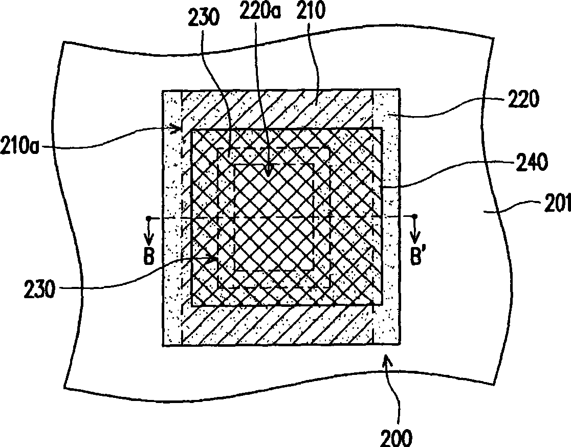
[0060] Figure 2A is a top view of a thin film diode according to an embodiment of the present invention, and Figure 2B for along Figure 2A The schematic cross-sectional view of the thin film diode shown by the section line BB'. Please also refer to Figure 2A and Figure 2B , the thin film diode 200 of this embodiment is suitable for disposing on a substrate 201 , wherein the thin film diode 200 includes a first electrode 210 , an insulating layer 220 , an active layer 230 and a second electrode 240 . The first electrode 210 is disposed on the substrate 201 . In this embodiment, the material of the substrate 201 can be selected from inorganic transparent materials (such as: glass, quartz, or other appropriate materials) or organic transparent materials (such as: polyolefins, polyols, polyalcohols, polyesters, etc.) polymers, rubber, thermoplastic polymers, thermosetting polymers, polyaromatic hydrocarbons, polymethylmethacrylates, polycarbonates, or other suitable mate...

no. 2 example

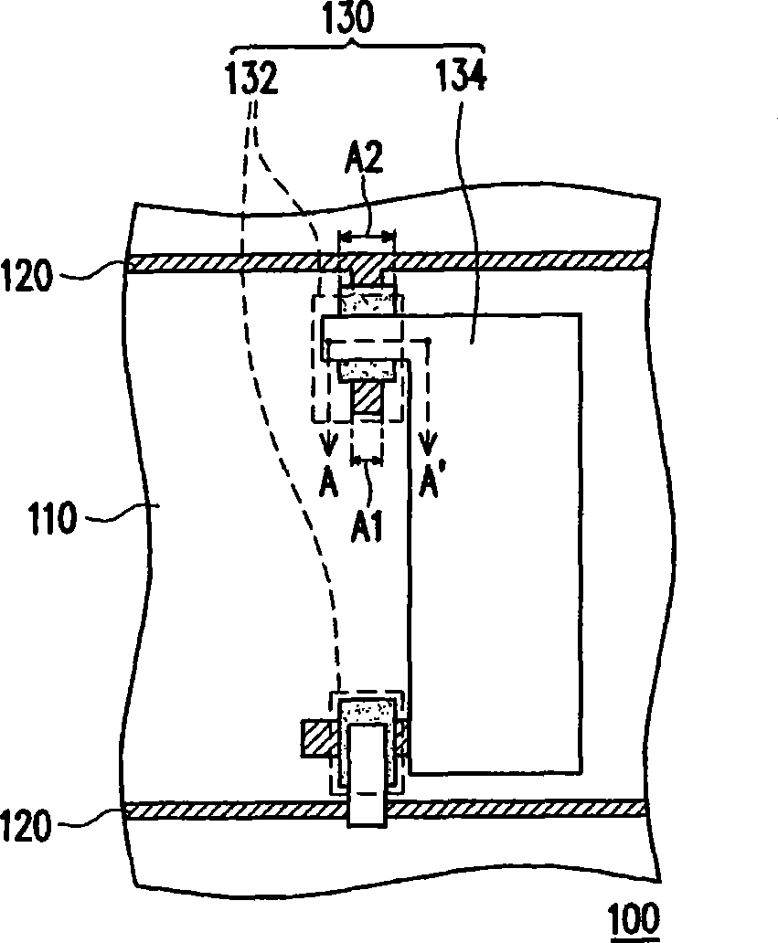
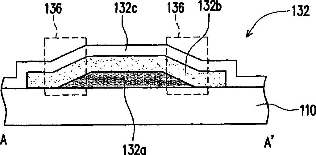
[0070] Figure 3A It is a schematic circuit diagram of a dual scanning diode array substrate according to an embodiment of the present invention, Figure 3B shown as Figure 3A The top view of the film layer in the region P1, while Figure 3C then along Figure 3B The cross-sectional schematic diagram shown by the section line CC'. Please also refer to Figure 3A , Figure 3B and Figure 3C , the dual scan diode array substrate 300 of this embodiment includes a substrate 310 , a plurality of scan lines 320 and a plurality of pixel units 330 . The scan lines 320 are disposed on the substrate 310 . The pixel units 330 are disposed on the substrate 310 , wherein each pixel unit 330 includes two thin film diodes 332 and a pixel electrode 334 . The pixel electrodes 334 are electrically connected to different scan lines 320 through the two thin film diodes 332 . Each thin film diode 332 adopts the film layer design of the above thin film diode 200 , and the same components ...


PUM


Abstract

The invention provides a thin-film diode, a dual scanning diode array substrate and a liquid crystal display panel, wherein the thin-film diode is suitable for being configured on a substrate. The thin-film diode comprises a first electrode, an insulating layer, an active layer and a second electrode, wherein the first electrode is configured on the substrate, the insulating layer is configured on the substrate so as to cover the first electrode, and the insulating layer is provided with an opening so as to expose the partial area of the first electrode; the active layer is configured on the first electrode, and extends to the insulating layer from the first electrode exposed through the opening; the second electrode is respectively configured on the insulating layer and the active layer; and the active layer is at least positioned in the coverage range of the second electrode. The invention also provides a liquid crystal display panel and a dual scanning diode array substrate with the thin-film diode.

Description

technical field [0001] The present invention relates to a diode, an array substrate and a display panel, and in particular to a thin-film diode (TFD), a dual selectdiode array substrate and a liquid crystal display panel. Background technique [0002] Generally speaking, a liquid crystal display panel is composed of a thin film transistor array substrate, a liquid crystal layer and a color filter substrate. Among them, the thin film transistor array substrate has a plurality of scanning lines, a plurality of data lines, a plurality of thin film transistors and a plurality of pixel electrodes, under proper control of the scanning lines and data lines, the image data can be smoothly transmitted to the Each pixel electrode, and through the voltage difference between each pixel and the common electrode on the color filter substrate, to achieve the purpose of image display. [0003] A general thin film transistor array substrate (TFT array substrate) generally requires five mask...

Claims


Application Information

Patent Timeline
Patent Type & Authority Applications(China)
IPC IPC(8): H01L29/861H01L29/43H01L27/12G02F1/1362
Inventor 吴岳鸿郭威宏陈政德周文彬李锡烈
Owner AU OPTRONICS CORP
Why Eureka
Try Eureka