Emitter circulating type solar cell and preparation thereof

A technology of emitter surround and solar cells, which is applied in the direction of photovoltaic power generation, circuits, electrical components, etc., can solve the problems of many through holes and complicated preparation process, and achieve the effect of simplifying the preparation process, reducing the number of through holes and improving mechanical strength

Inactive Publication Date: 2009-03-11
INST OF ELECTRICAL ENG CHINESE ACAD OF SCI +1
View PDF3 Cites 14 Cited by
  • Summary
  • Abstract
  • Description
  • Claims
  • Application Information

AI Technical Summary

Problems solved by technology

[0004] The purpose of the present invention is to overcome the shortcomings of too many through holes in the prior art of EWT solar cells and the preparation process is too complicated, and provide EWT solar cells and its preparation method

Method used


Image

  • Emitter circulating type solar cell and preparation thereof
  • Emitter circulating type solar cell and preparation thereof
  • Emitter circulating type solar cell and preparation thereof

Examples


Embodiment 1

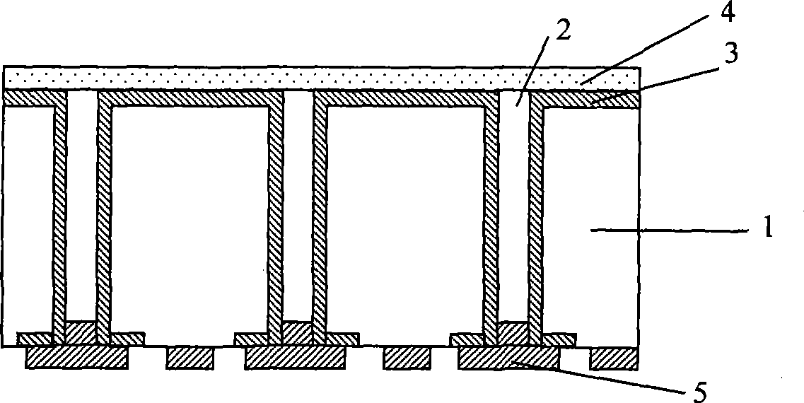
[0058] combined with figure 2 , 4 , 5, a kind of EWT solar cell provided by the present embodiment is as follows: the silicon chip 1 is a p-type silicon chip, and the interior contains an array of through holes 2 that run through the silicon chip 1 arranged in a hexagonal lattice, and the diameter of the through holes 2 is 50 μm, and the interval between adjacent through holes 2 is 0.5 mm. An n-type lightly doped emitter 3 is contained on the light-facing surface of the silicon wafer 1 and in the through hole 2 , and the sheet resistance of the lightly doped emitter 3 is 150Ω / □. A passivation medium layer 4 is deposited on the lightly doped emitter 3, and the passivation medium layer 4 is a silicon nitride film with a thickness of 80nm. There is an n-type heavily doped emitter 6 on the backlight surface of the silicon wafer 1, and the through hole 2 on the backlight surface of the silicon wafer 1 is in the pattern of the heavily doped emitter 6, and the heavily doped emitte...

Embodiment 2

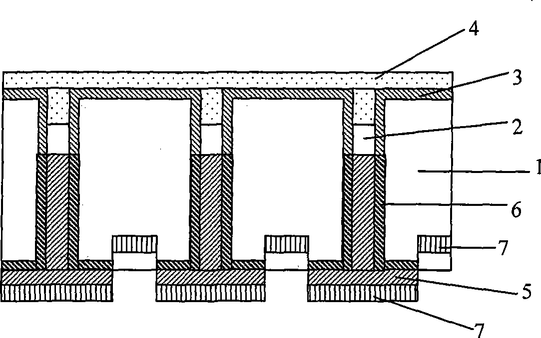
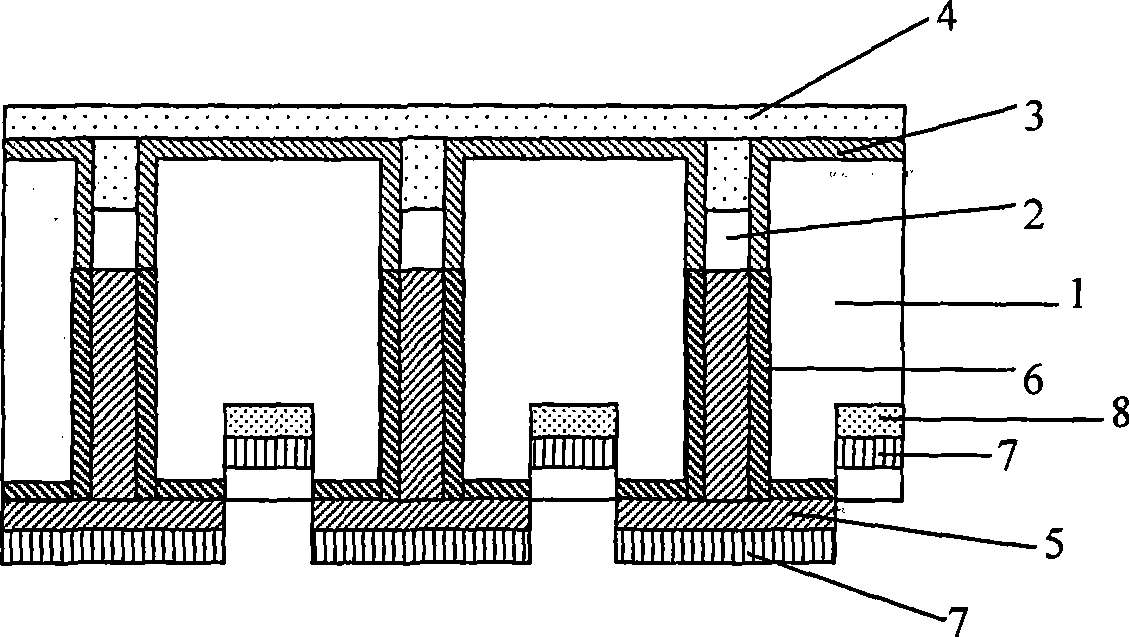
[0060] combined with image 3 , 4 , 5. The EWT solar cell provided in this embodiment is as follows: the silicon wafer 1 is an n-type silicon wafer, which contains an array of through holes 2 that run through the silicon wafer 1 arranged in a hexagonal lattice, and the diameter of the through holes 2 is 50 μm. The interval between adjacent through holes 2 is 1.5mm. There is a p-type lightly doped emitter 3 on the light-facing surface of the silicon wafer 1 and in the through hole 2 , and the sheet resistance of the lightly doped emitter 3 is 100Ω / □. A passivation medium layer 4 is deposited on the lightly doped emitter 3, and the passivation medium layer 4 is a silicon nitride film with a thickness of 80nm. There is a p-type heavily doped emitter 6 on the backlight surface of the silicon wafer 1, and the through hole 2 on the backlight surface of the silicon wafer 1 is in the pattern of the heavily doped emitter 6, and the heavily doped emitter 6 partially enters the throug...

Embodiment 3

[0062] Such as Figure 6 As shown, the present embodiment is a method for preparing the EWT solar cell, and the main steps include in order:

[0063] Step 1: Provide a p-type silicon wafer 1, the silicon wafer 1 has a light facing surface and a backlight surface, and an array of through holes 2 penetrating the silicon wafer is prepared on the silicon wafer 1 by a laser etching process, and the through holes 2 are 50 μm in diameter;

[0064] Step 2: pickling and rinsing with deionized water to clean the silicon wafer 1 prepared with through holes 2;

[0065] Step 3: POCl using a diffusion furnace 3 Diffusion, forming an n-type lightly doped emitter 3 on the light-receiving surface, the backlight surface and the inside of the through hole 2 of the silicon wafer 1, and the sheet resistance of the lightly doped emitter 3 is 130Ω / □;

[0066] Step 4: Deposit a silicon nitride film with a thickness of 80 nm on the light-facing surface of the silicon wafer 1 as a passivation dielec...


PUM


Abstract

The invention relates to a surrounding-emitting electrode solar cell and a preparation method thereof. The cell contains arrays which are arranged in a hexagonal lattice way and penetrate through holes 2 of an irradiation surface and a backlight surface of a silicon chip 1 in the silicon chip 1, therefore, the quantity of the through holes is minimized, and the breakage ratio of the silicon chip in the process of the hole drilling technology is reduced; a heavily doped emitting electrode 6 included on the back surface of the silicon chip 1 partially enters into the through holes, and a first conductive metal electrode 5 is arranged on the heavily doped emitting electrode 6, and plays the role of collecting minority carriers. A groove is arranged at the circumference of the first conductive metal electrode 5 by etching, a second conductive metal electrode 7 is arranged in the groove and plays the role of collecting majority carriers, and the first conductive metal electrode 5 and the second conductive metal electrode 7 deposited in the groove are insulated and isolated through the step of the groove.

Description

technical field [0001] The invention relates to a solar cell and a preparation method thereof, in particular to an emitter wrap-around (EWT) solar cell and a preparation method of the solar cell. Background technique [0002] Back contact silicon solar cells have several advantages over conventional silicon solar cells. The first advantage is that back-contact cells have higher conversion efficiencies due to reduced or eliminated shading losses of the contact grid (sunlight reflected from the grid cannot be converted into electrical current). A second advantage is that since the contact areas for both polarities are made on the backlight side, back-contact cells are easier to assemble into circuits and are therefore less expensive. Back contact cells also have a more uniform appearance and thus better aesthetics. [0003] There are several methods for fabricating back-contact silicon solar cells. These methods include metallization wrap around (MWA), metallization wrap ar...

Claims


Application Information

Patent Timeline
Patent Type & Authority Applications(China)
IPC IPC(8): H01L31/06H01L31/0224H01L31/18
CPCH01L31/022458H01L31/022433Y02E10/50
Inventor 赵雷王文静
Owner INST OF ELECTRICAL ENG CHINESE ACAD OF SCI
Why Eureka
Try Eureka