Method for on-line measurement of MEMS membrane stress gradient

A thin-film stress and thin-film technology, which is applied in the field of online measurement of micro-electromechanical system thin-film stress gradient, can solve the problems of affecting measurement accuracy, measurement accuracy error, and width cannot be accurately controlled.

Inactive Publication Date: 2009-04-08
CHANGSHU NANJING NORMAL UNIV DEV RES INST
View PDF0 Cites 21 Cited by
  • Summary
  • Abstract
  • Description
  • Claims
  • Application Information

AI Technical Summary

Problems solved by technology

If you choose a wider cantilever beam as the test structure, the deflection in the width direction will affect the measurement accuracy; if you choose a narrow beam or Archimedes spiral structure, the width cannot be accurately controlled during etching, and the interface along the width direction is not ideal rectangle, these will cause significant error to the measurement accuracy

Method used


Image

  • Method for on-line measurement of MEMS membrane stress gradient
  • Method for on-line measurement of MEMS membrane stress gradient
  • Method for on-line measurement of MEMS membrane stress gradient

Examples


Embodiment

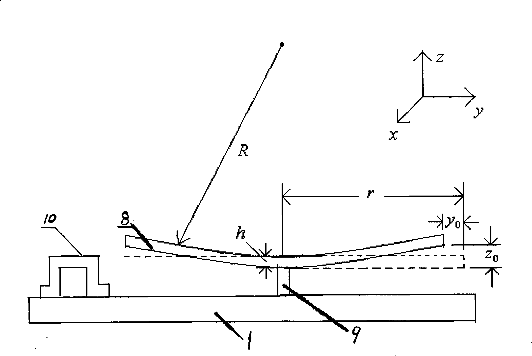
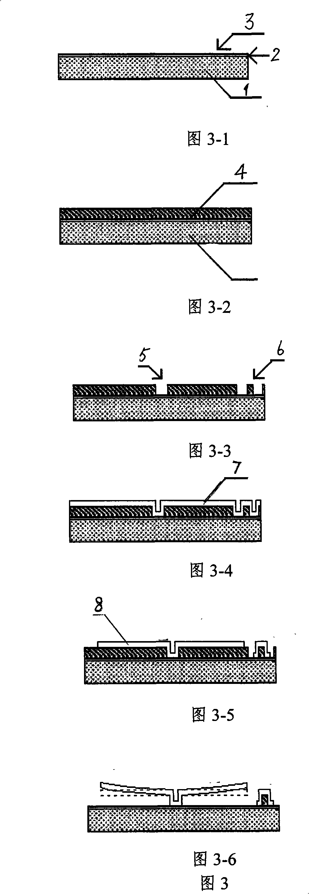
[0041] As shown in Figure 3-1, in the silicon sacrificial layer MEMS process, a thin layer of SiO is deposited on the single crystal silicon substrate 1 by LPCVD (low pressure chemical vapor deposition) method. 2 2. Deposit a layer of silicon nitride 3 with a thickness of 0.2 μm, and then deposit a layer of phosphosilicate glass with a thickness of 2 μm as the sacrificial layer 4 (Figure 3-2), and use KOH solution to carve on the sacrificial layer 4 of phosphosilicate glass. Etching a circular cavity 5 with a diameter of 4 μm is used as an anchor region 9, and a ring 6 is used as a reference surface 10 (the distance between the two is slightly greater than 100 μm) (Figure 3-3), and then deposited with polysilicon A thin film with a thickness of h=1 μm is used as the structural layer 7 (Figure 3-4). On the structural layer, take the center of the anchor region as the center, etch a circle with a radius of r=50 μm as the fixed circular thin film 8 at the center, and The periphe...


PUM


Abstract

The invention discloses a method used for online measuring the stress gradient of MEMS film, comprising the steps as follows: a round film with center fixed is prepared on a structure layer film; after the round film is released, the round film generates deformation under the stress gradient inside the round film; the displacement of the edge of the round film in the vertical direction is measured by a non-contact phase-shifting typed Mirau interferometer, thus calculating the curvature radius of the round film; and the stress gradient of the film can be calculated by the young modulus and Poisson ratio of the film and the curvature radius of the round film. The measurement method is characterized in that a centrosymmetric round film with the center fixed is used as a testing structure and a choring area is fixedly clamped closely to an ideal state, thus improving the precision of the model; the non-contact optical interference method is used for measurement, thus not affecting testing structure and having good repeatability; the method is suitable for measuring the stress gradient of conductive material and non-conductive material simultaneously; and furthermore, the measurement method has the advantages of simple and convenient operation, high measurement precision, small chip occupying area and the like.

Description

technical field [0001] The invention relates to a method capable of online measuring the stress gradient of a microelectromechanical system (MEMS) film, and belongs to the technical field of MEMS material parameter measurement. Background technique [0002] The application fields of MEMS technology are very broad, and can be used in many fields such as inertial measurement, microfluidics, optics (optical switches, display devices, etc.), pressure measurement, and RF devices. [0003] Film deposition is an important process step in the processing of silicon-based MEMS (microelectro-mechanical systems) devices, but due to unfavorable factors such as lattice mismatch, different thermal expansion coefficients between the structural layer and the substrate material, residual stress and Stress gradient in the thickness direction. [0004] The stress gradient will cause the deformation of the film and reduce the performance of the MEMS device. Excessive stress gradient can even ca...

Claims


Application Information

Patent Timeline
Patent Type & Authority Applications(China)
IPC IPC(8): G01N21/45G01N19/00
Inventor 戎华陈涵王鸣
Owner CHANGSHU NANJING NORMAL UNIV DEV RES INST
Why Eureka
Try Eureka