Pellicle and method for manufacturing the same

A technology of protective film and manufacturing method, which is applied in the direction of semiconductor/solid-state device manufacturing, electrical components, photoplate making process of pattern surface, etc., can solve the problems of optical film characteristic degradation and unevenness, and achieve excellent high light transmittance and The effect of chemical stability

Inactive Publication Date: 2009-04-22
SHIN ETSU CHEM IND CO LTD
View PDF1 Cites 13 Cited by
  • Summary
  • Abstract
  • Description
  • Claims
  • Application Information

AI Technical Summary

Problems solved by technology

[0009] Furthermore, as in the pellicle film disclosed in Patent Document 1 or Non-Patent Document 1, strong stress is easily introduced in

Method used


Image

  • Pellicle and method for manufacturing the same
  • Pellicle and method for manufacturing the same
  • Pellicle and method for manufacturing the same

Examples


Embodiment 1

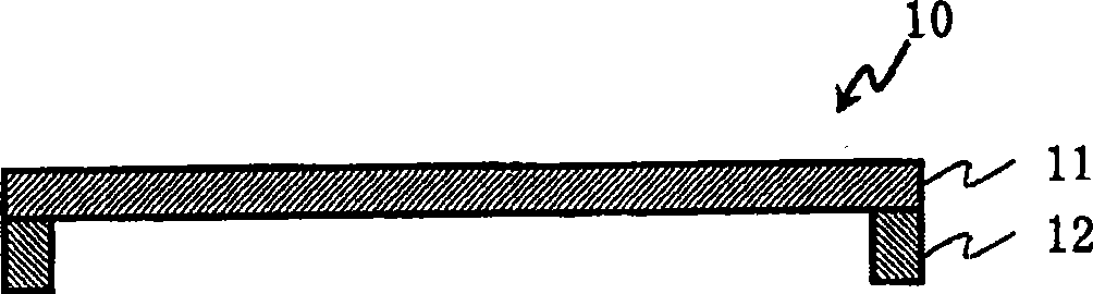
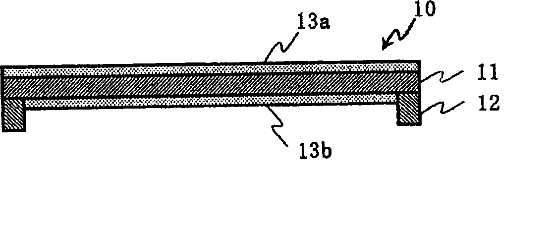
[0057] Fig. 3 is a process explanatory diagram for explaining the method of manufacturing the pellicle assembly of the present invention. The support substrate 1 of the SOI (Silicon On Insulator) substrate shown in FIG. 3(A) is a substrate with an oxide film 1b on the surface of the silicon substrate 1a, the SOQ (Silicon On Quartz) substrate and the SOG (Silicon On Glass) substrate The supporting substrate 1 is a quartz substrate and a glass substrate, respectively. A single crystal silicon crystal film 2 is provided on the main surfaces of the support substrates 1, and the silicon crystal film 2 becomes a protective film.

[0058] The silicon substrate 1a as the support substrate of the SOI substrate is, for example, a generally commercially available single crystal silicon substrate made by the czochralski method (CZ method). On the surface of the single crystal silicon substrate 1a, An oxide film 1b having a thickness of about 100 nm is formed in advance by a method such as the...

Embodiment 2

[0067] The silicon crystal film 11 supported by the pellicle frame 12 is produced according to the steps shown in FIG. 3. In addition, the thickness of the silicon crystal film 11 of this embodiment is 20 nm. Then, on the surface and bottom surface of the silicon crystal film 11, a SiC thin film with a thickness of several nanometers is vapor-deposited on the silicon crystal film by a gas clustering and ion beam evaporation method to cover the silicon crystal film.

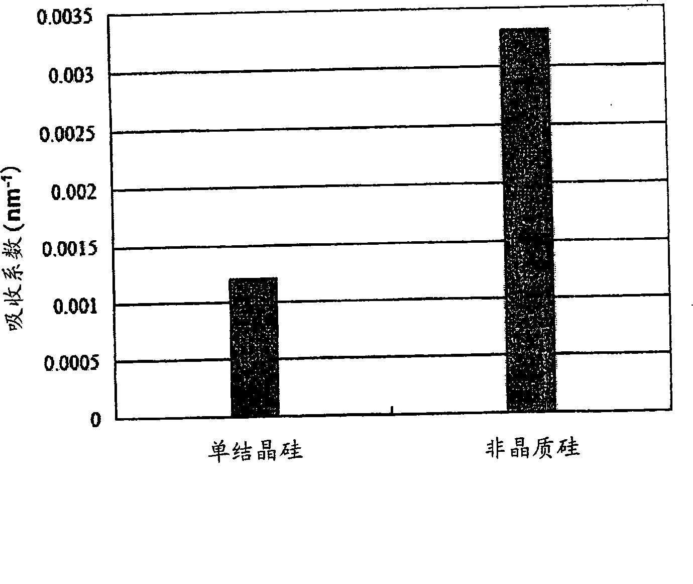
[0068] The pellicle components obtained in Example 1 and Example 2 have EUV light transmittance above 50%, and the throughput per unit time during EUV exposure can reach a practical level, and the device has no yield rate due to foreign matter. The reduced situation occurs.

[0069] According to the present invention, a protective film component can be provided, which has a practical protective film for EUV, which has excellent high light transmittance and chemical stability.


PUM

PropertyMeasurementUnit
Thicknessaaaaaaaaaa
Thicknessaaaaaaaaaa

Abstract

The present invention relates to a pellicle. It is therefore an object of the present invention to provide a pellicle provided with a practical pellicle film for EUV superior in transmittance and chemical stability. A pellicle of the present invention is provided with a silicon crystal film, the absorption coefficient of which is 0.005/nm or lower with respect to light having a wavelength of 13.5 nm, as a pellicle film. The silicon crystal film is an indirect transition type semiconductor film and, therefore, the optical absorption coefficient thereof is relatively low. In particular, a single-crystal silicon film has a lower absorption coefficient than an amorphous silicon film and a polysilicon film. Thus, it is easy to obtain desired transmissivity required of a pellicle film for EUV from the single-crystal silicon film. Such a pellicle film as described above can be fabricated from an SOI film obtained by thin-filming an SOI substrate (including an SOQ substrate and an SOG substrate). If a pellicle film of the silicon crystal film is made from the SOI film, no excessive stress is subjected in the pellicle film formation process, and the pellicle film is formed under room temperature without causing strains.

Description

Technical field [0001] The present invention relates to a protective film component for lithography, and more specifically, to a protective film component suitable for extreme ultraviolet (EUV: Extreme Ultra Violet) lithography process and its manufacturing method. Background technique [0002] As semiconductor devices become highly integrated, the patterns formed by lithography are also becoming miniaturized, and devices with a pattern width of about 45 nm are now entering the practical stage. Such a fine line pattern can be realized by using ArF immersion exposure method or double exposure method for lithography, which is an improved technique of conventional excimer exposure technology. [0003] However, lithography based on these excimer exposure technologies cannot cope with the requirements for finer patterns, such as those with a width below 32nm. Therefore, the new exposure technology uses extreme ultraviolet (EUV: Extreme Ultra Violet) Micro-imaging began to receive atte...

Claims


Application Information

Patent Timeline
IPC IPC(8): G03F1/14G03F1/62H01L21/027
Inventor 久保田芳宏秋山昌次进藤敏彦
Owner SHIN ETSU CHEM IND CO LTD
Why Eureka
Try Eureka