Method for preparing high-density silicon nano-crystalline film

A silicon nanocrystal, high-density technology, applied in semiconductor/solid-state device manufacturing, electrical components, circuits, etc., to achieve multi-purpose and simple process steps

Inactive Publication Date: 2009-04-22
SEMICON MFG INT (SHANGHAI) CORP +1
View PDF0 Cites 12 Cited by
  • Summary
  • Abstract
  • Description
  • Claims
  • Application Information

AI Technical Summary

Problems solved by technology

[0007] The main purpose of the present invention is to overcome the defects existing in the preparation method of the existing silicon nanocrystal film, and provide a new preparation method of the high-density silicon nanocrystal film, the technical problem to be solved is to make it evaporat...

Method used


Image

  • Method for preparing high-density silicon nano-crystalline film
  • Method for preparing high-density silicon nano-crystalline film
  • Method for preparing high-density silicon nano-crystalline film

Examples


Embodiment Construction

[0030] For further elaborating the technical means and effect that the present invention takes for reaching the intended invention purpose, below in conjunction with accompanying drawing and preferred embodiment, to its specific implementation, structure , features and their effects are described in detail below.

[0031] In order to make the object, technical solution and advantages of the present invention clearer, the present invention will be described in further detail below in conjunction with specific embodiments and with reference to the accompanying drawings.

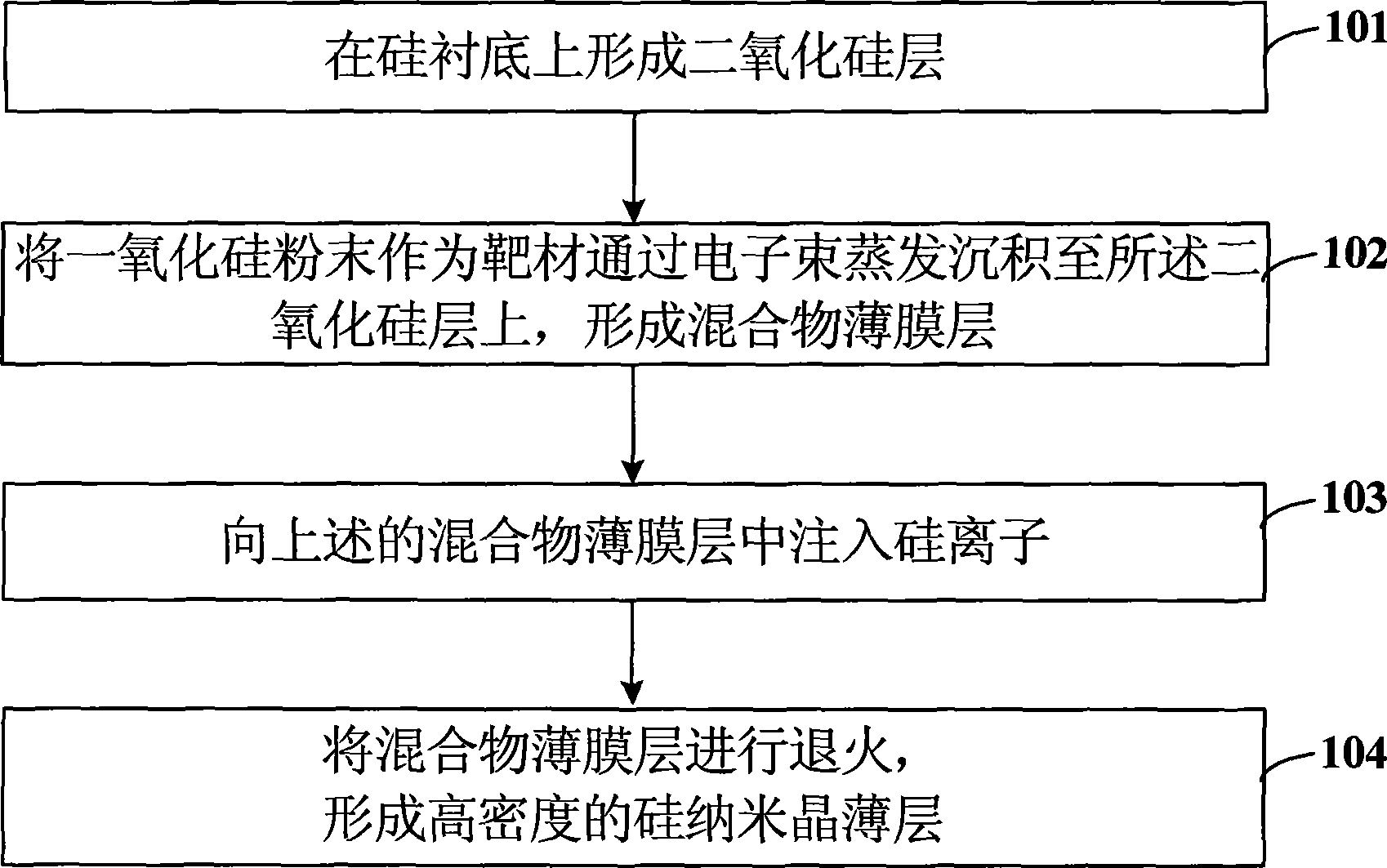
[0032] Such as figure 1 as shown, figure 1 It is a flow chart of a method for preparing a silicon nanocrystal film provided by the invention, the method comprising the following steps:

[0033] Step 101: Thermally grow a silicon dioxide layer on a silicon substrate. The silicon substrate is a flat and clean low-resistance silicon substrate, a high-resistance silicon substrate, or a silicon-on-insulator (SOI)...


PUM


Abstract

The invention relates to a preparation method of a high-density silicon nano-crystalline thin film, and the preparation method comprises: a silicon dioxide layer is formed on a silicon substrate; silicon monoxide is taken as a target material to be deposited on the silicon dioxide layer by the electron beam evaporation method, thereby forming a mixture thin film layer; silicon ions are implanted in the mixture thin film layer; and the mixture thin film layer is annealed to form the high-density silicon nano-crystalline thin film layer. The preparation method prepares the high-density silicon nano-crystalline thin film by the electron beam evaporation of the silicon monoxide and the ion implantation method for matching, thereby having the advantages of simple process steps, multiple purposes and ability of being compatible with the traditional Si-based CMOS technology. The surface density of the silicon nano-crystalline which is prepared by using the method can be up to 10<12>cm<minus 1> level, and the diameter of particles is in the range of 5-8nm. The preparation method is mainly applied in the preparation of key components of the third generation of silicon-based solar cell chips, silicon single electron devices, single electron memories, silicon nano-crystalline floating gate memories and other aspects, thereby being applicable to the requirements on large-scale production.

Description

technical field [0001] The invention relates to the technical field of nano-semiconductor processing, in particular to a method for preparing a high-density silicon nanocrystal thin film using an electron beam evaporation method combined with an ion implantation method. Background technique [0002] Silicon nanocrystalline thin film layer is an important and core component of optoelectronic devices and nanoelectronic devices. Such devices include: third-generation nanocrystalline solar cell chips, silicon single-electron devices, single-electron memories, etc. [0003] First of all, nanostructures are gradually becoming the protagonists in optoelectronic components, taking the third-generation solar cells as an example. On the road of constant pursuit of high efficiency and low cost, people never stop moving forward. The bulk silicon material used in the first generation of silicon-based solar cells has been replaced by Thin Film Solar Cell (Thin Film Solar Cell) materials...

Claims


Application Information

Patent Timeline
IPC IPC(8): H01L21/00H01L21/20
Inventor 陈晨贾锐李维龙朱晨昕李昊峰刘明田继红路程
Owner SEMICON MFG INT (SHANGHAI) CORP
Why Eureka
Try Eureka