Production process for golden electrode for LED
A technology of light emitting diodes and gold electrodes is applied in the field of preparation of light emitting diode gold electrodes to achieve the effects of no pinhole cracks, stable storage and bright surface.
- Summary
- Abstract
- Description
- Claims
- Application Information
AI Technical Summary
Problems solved by technology
Method used
Image

Examples
Embodiment 1
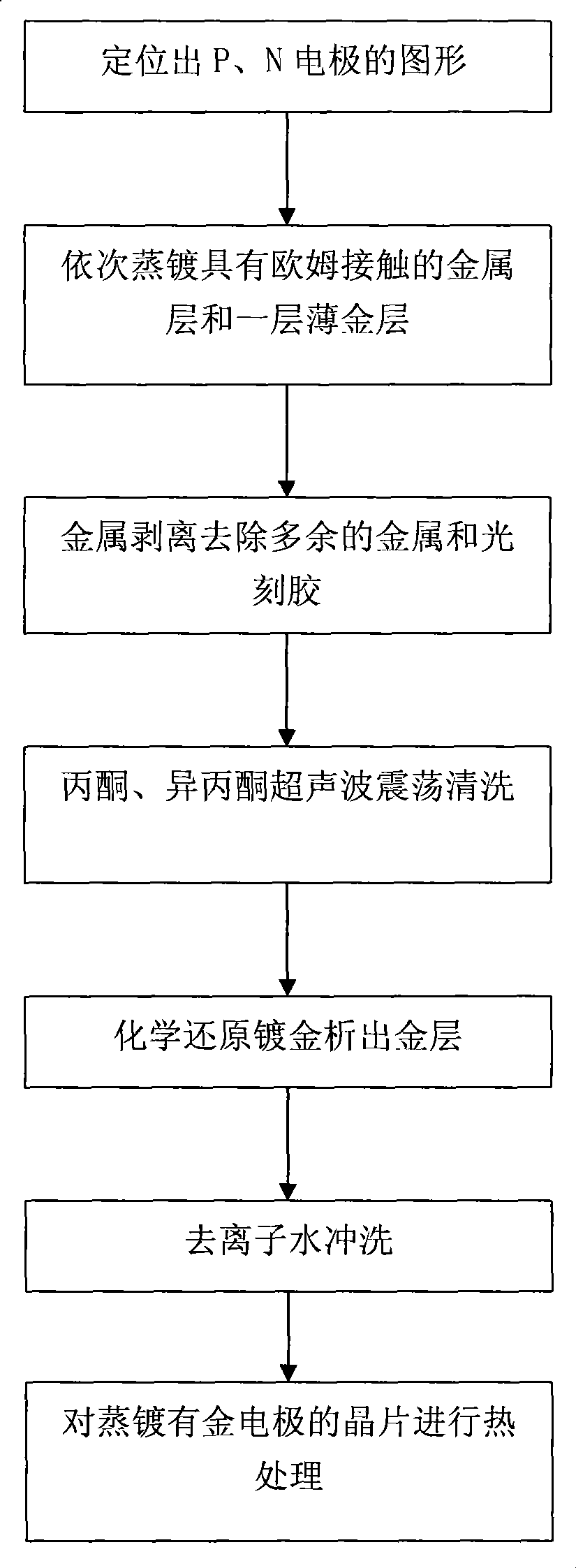
[0041] Such as figure 1 As shown, the preparation method of the light-emitting diode gold electrode of the present embodiment 1 comprises the following steps:
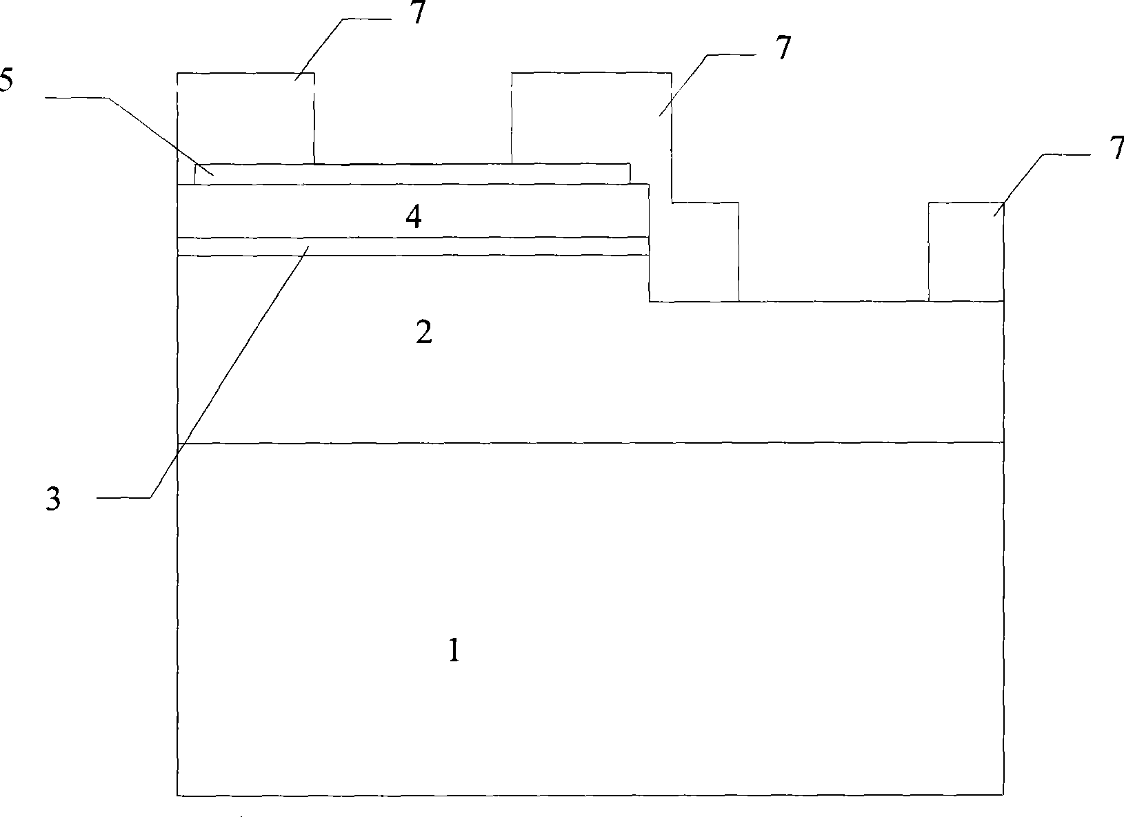
[0042] (1) epitaxially growing N-type layer 2, active layer 3, and P-type layer 1 on sapphire substrate 1; etching N-type layer 2 with a plasma etching machine, and vapor-depositing P-type layer transparent conductive layer 5; Transfer the pattern of the P and N electrode masks to the photoresist 7 on the chip surface by photolithography, such as figure 2 shown;
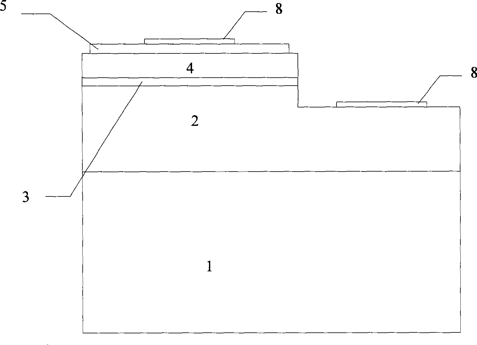
[0043] (2) On the transparent electrode layer 5, the N-type layer 2, the metal layer with ohmic contact and a layer of gold 8 with a thickness of 300 angstroms are evaporated successively, as image 3 Shown; remove excess photoresist and metal by Lift-off, then clean the wafer with acetone and isopropanone ultrasonic vibration to remove residual photoresist and organic matter;
[0044] (3) Under the conditions of 5g / L of gold sodium sulfite (calculated as...
Embodiment 2
[0048] Such as figure 1 As shown, the preparation method of the light-emitting diode gold electrode of the present embodiment 2 comprises the following steps:
[0049] (1) epitaxially growing N-type layer 2, active layer 3, and P-type layer 1 on sapphire substrate 1; etching N-type layer 2 with a plasma etching machine, and vapor-depositing P-type layer transparent conductive layer 5; Transfer the pattern of the P and N electrode masks to the photoresist 7 on the chip surface by photolithography, such as figure 2 shown;
[0050] (2) On the transparent electrode layer 5, the N-type layer 2, the metal layer with ohmic contact and a layer of gold 8 with a thickness of 500 angstroms are evaporated successively, as image 3Shown; remove excess photoresist and metal by Lift-off, then clean the wafer with acetone and isopropanone ultrasonic vibration to remove residual photoresist and organic matter;
[0051] (3) Under the conditions of 5 g / L of sodium gold sulfite (calculated as...
Embodiment 3
[0055] Such as figure 1 As shown, the preparation method of the light-emitting diode gold electrode of the present embodiment 3 comprises the following steps:
[0056] (1) epitaxially grow N-type layer 2, active layer 3, and P-type layer 4 on sapphire substrate 1; etch out N-type layer 2 with a plasma etching machine, and vapor-deposit P-type layer transparent conductive layer 5 and Silicon dioxide protective layer 6; transfer the image of the P and N electrode mask plates to the photoresist 7 on the chip surface by photolithography, and etch and remove the silicon dioxide at the electrode position, such as Figure 5 shown;
[0057] (2) On the transparent electrode layer 5, the N-type layer 2, the metal layer with ohmic contact and a layer of gold 8 with a thickness of 400 angstroms are evaporated successively, as Figure 6 Shown; remove excess photoresist and metal by Lift-off, then clean the wafer with acetone and isopropanone ultrasonic vibration to remove residual photor...
PUM
| Property | Measurement | Unit |
|---|---|---|
| thickness | aaaaa | aaaaa |
| thickness | aaaaa | aaaaa |
| hardness | aaaaa | aaaaa |
Abstract
Description
Claims
Application Information
 - R&D
- Intellectual Property
- Life Sciences
- Materials
- Tech Scout
- Unparalleled Data Quality
- Higher Quality Content
- 60% Fewer Hallucinations
Browse by: Latest US Patents, China's latest patents, Technical Efficacy Thesaurus, Application Domain, Technology Topic, Popular Technical Reports.
© 2025 PatSnap. All rights reserved.Legal|Privacy policy|Modern Slavery Act Transparency Statement|Sitemap|About US| Contact US: help@patsnap.com