Production method for organic thin-film transistor with graphic active layer

An organic thin-film, patterning technology, applied in semiconductor/solid-state device manufacturing, semiconductor devices, electric solid-state devices, etc., can solve problems such as performance degradation, organic thin-film performance damage, and manufacturing process limitations

Active Publication Date: 2009-04-29
SEMICON MFG INT (SHANGHAI) CORP +1
View PDF0 Cites 5 Cited by
  • Summary
  • Abstract
  • Description
  • Claims
  • Application Information

AI Technical Summary

Problems solved by technology

[0003] In traditional microelectronics processing, photolithography is generally used to pattern the semiconductor layer of silicon thin film transistors, but this method cannot be directly applied to the patterning of organic semiconductor thin films, because various Both the solution and the photoresist itself will damage the properties of the organic film
[0004] Jackson's research group has developed a method (Appl.Phys.Lett., 74, 3302, 1999) for patterning the active layer using polyvinyl alcohol (PVA) as a negative glue and a protective layer, but the yield is low
Ali Afzali et al. (IBM, Adv.Mater., 15, 2066, 2003) used a solution processing method to pattern the active layer, but after the device passed through the solvent, the performance decreased significantly
Jin Jiang et al proposed to pattern the active layer with a self-organization method, but the repeatability is not good
Stijn De Vusser et al. (Appl. Phys. Lett., 88, 103501, 2006) thought of using photoresist as a mask (integrated shadow mask) to pattern the active layer, but the photoresist in this method It cannot be removed, so that the subsequent manufacturing process is subject to certain restrictions

Method used


Image

  • Production method for organic thin-film transistor with graphic active layer
  • Production method for organic thin-film transistor with graphic active layer
  • Production method for organic thin-film transistor with graphic active layer

Examples


Embodiment Construction

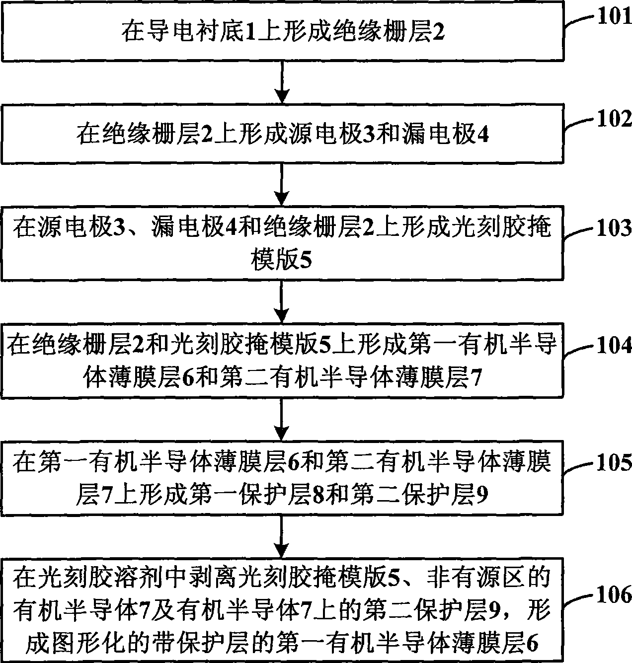
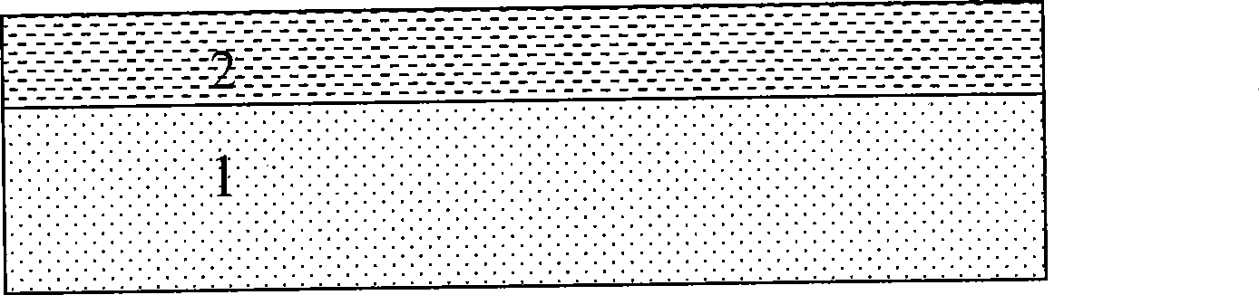
[0034] In order to make the object, technical solution and advantages of the present invention clearer, the present invention will be described in further detail below in conjunction with specific embodiments and with reference to the accompanying drawings.

[0035] The core content of the present invention is: after the preparation of the metal source and drain electrodes, the photoresist is used as a mask, and the organic semiconductor thin film layer is prepared by vacuum evaporation method, and then a layer of organic semiconductor thin film layer is prepared by room temperature PECVD method on the organic semiconductor thin film layer. protective layer, and make the sum of the organic semiconductor thin film layer and the protective layer thickness less than the thickness of the metal source drain electrode, to ensure that the glue remover does not contact the organic semiconductor thin film layer when removing the photoresist mask, causing the Destruction of the propertie...


PUM


Abstract

The invention relates to the technical field of organic semiconductor devices and micro processing and discloses a method for preparing an active patternized organic thin-film transistor. The method adopts a photoresist as a mask after the preparation of a metal source-drain electrode. Firstly an organic semiconductor thin film layer is prepared with a vacuum vaporization method. Then a room temperature PECVD method is adopted to prepare a protective layer on the organic semiconductor thin film layer. The total thickness of the organic semiconductor thin film layer and the protective layer is smaller than the thickness of the metal source-drain electrode to ensure that a resist remover does not contact the organic semiconductor thin film layer so as to cause damage to the performance of the organic semiconductor thin film layer when the photoresist mask is removed. The invention can be completely compatible with the traditional IC process. The prepared active patternized organic thin-film transistor has the properties of small off-state current and high ratio of current switching.

Description

technical field [0001] The invention relates to the technical field of organic semiconductor devices and microfabrication, in particular to a method for preparing an organic thin film transistor with a patterned active layer. Background technique [0002] With the development of the organic electronics industry, organic thin film transistors have shown great application potential in flexible active matrix displays and flexible integrated circuits. Patterning the active layer is an essential step to realize organic semiconductor applications. [0003] In traditional microelectronics processing, photolithography is generally used to pattern the semiconductor layer of silicon thin film transistors, but this method cannot be directly applied to the patterning of organic semiconductor thin films, because various Both the solution and the photoresist itself will damage the properties of the organic film. [0004] Jackson's research group has developed a method (Appl.Phys.Lett., ...

Claims


Application Information

Patent Timeline
Patent Type & Authority Applications(China)
IPC IPC(8): H01L51/40
Inventor 甄丽娟商立伟刘明
Owner SEMICON MFG INT (SHANGHAI) CORP
Why Eureka
Try Eureka