

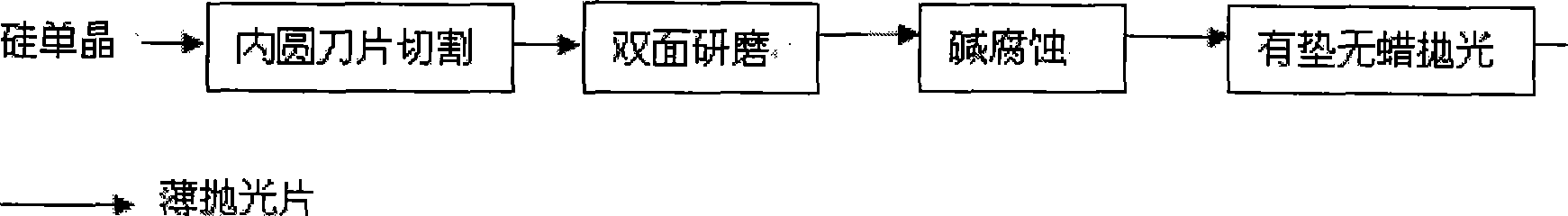
Processing method of thin silicon monocrystal polished section
A processing method and technology of silicon single crystal, applied in electrical components, semiconductor/solid-state device manufacturing, circuits, etc., can solve the problems of large amount of throwing, complicated process, can not meet user requirements, etc., and achieve the effect of improving productivity and quality
- Summary
- Abstract
- Description
- Claims
- Application Information
AI Technical Summary
Problems solved by technology
Method used
Image

Examples
Embodiment Construction
[0020] The contents, advantages and objects of the present invention will be set forth in the following description of the embodiments.
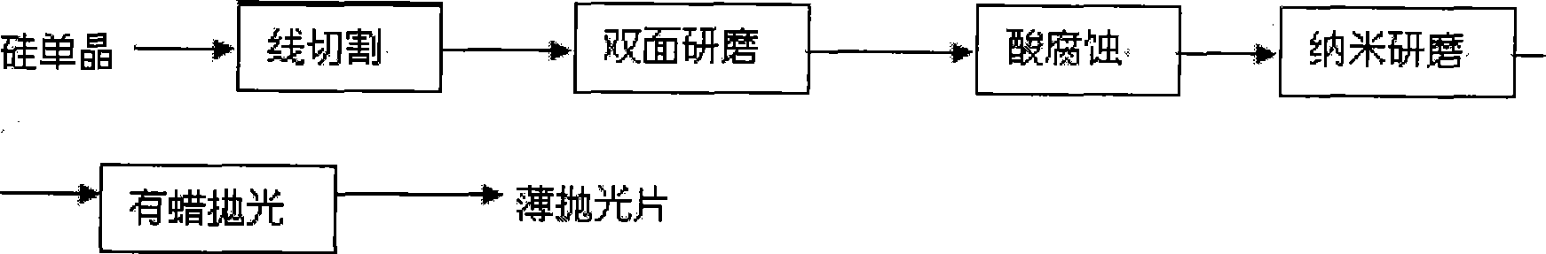
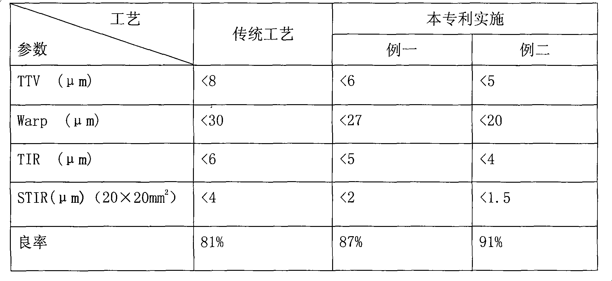
[0021] Embodiment 1 of this patent is processing a 6-inch heavily arsenic-doped N-type polished silicon wafer.
[0022] In the acid corrosion thinning process, the volume ratio of the mixed acid solution (nitric acid, hydrofluoric acid and buffer acid such as phosphoric acid, glacial acetic acid, etc.) is 2:1:1, the corrosion temperature is 40°C, the corrosion time is 30 seconds, and the acid corrosion removal amount 33 microns; the concentration of weak alkaline cleaning agent is 4%, the cleaning temperature is 60°C, the ultrasonic time is 5 minutes, and the rinsing time is 5 minutes. In the nano-grinding process, the spindle rotation speed of the nano-grinding machine is 4800 rpm, the feed speed of the spindle is 0.8 μm / s, the rotation speed of the ceramic disc is 20 rpm, and the removal amount of the nano-grinding is 6 μm. In the polish...
PUM
 Abstract
Description
Claims
Application Information