Double-surface position alignment apparatus and method

A technology for aligning devices and surface positions, which is applied in the photolithographic process exposure device, pattern surface photographic process, optics, etc., can solve the problems of increased design complexity, inability to align field by field, poor process adaptability, etc. Achieve the effects of reducing design complexity and structural design complexity, reducing processing and manufacturing costs, and improving process adaptability

Active Publication Date: 2009-05-20
SHANGHAI MICRO ELECTRONICS EQUIP (GRP) CO LTD
View PDF0 Cites 31 Cited by
  • Summary
  • Abstract
  • Description
  • Claims
  • Application Information

AI Technical Summary

Problems solved by technology

However, the above two silicon wafer back position alignment methods mainly have the following disadvantages in structural realization: the alignment light source is visible light, and the optical projection objective is required to be achromatic in the visible light alignment band or the alignment device is required to be aligned with the optical projection objective. Compensation for the chromatic aberration generated by the wave band, which will increase the complexity of the design of the optical projection objective lens or the position alignment device and increase the design cost; two sets of optical path turning systems are installed at the bottom ends of both sides of the silicon w

Method used


Image

  • Double-surface position alignment apparatus and method
  • Double-surface position alignment apparatus and method
  • Double-surface position alignment apparatus and method

Examples


Example Embodiment

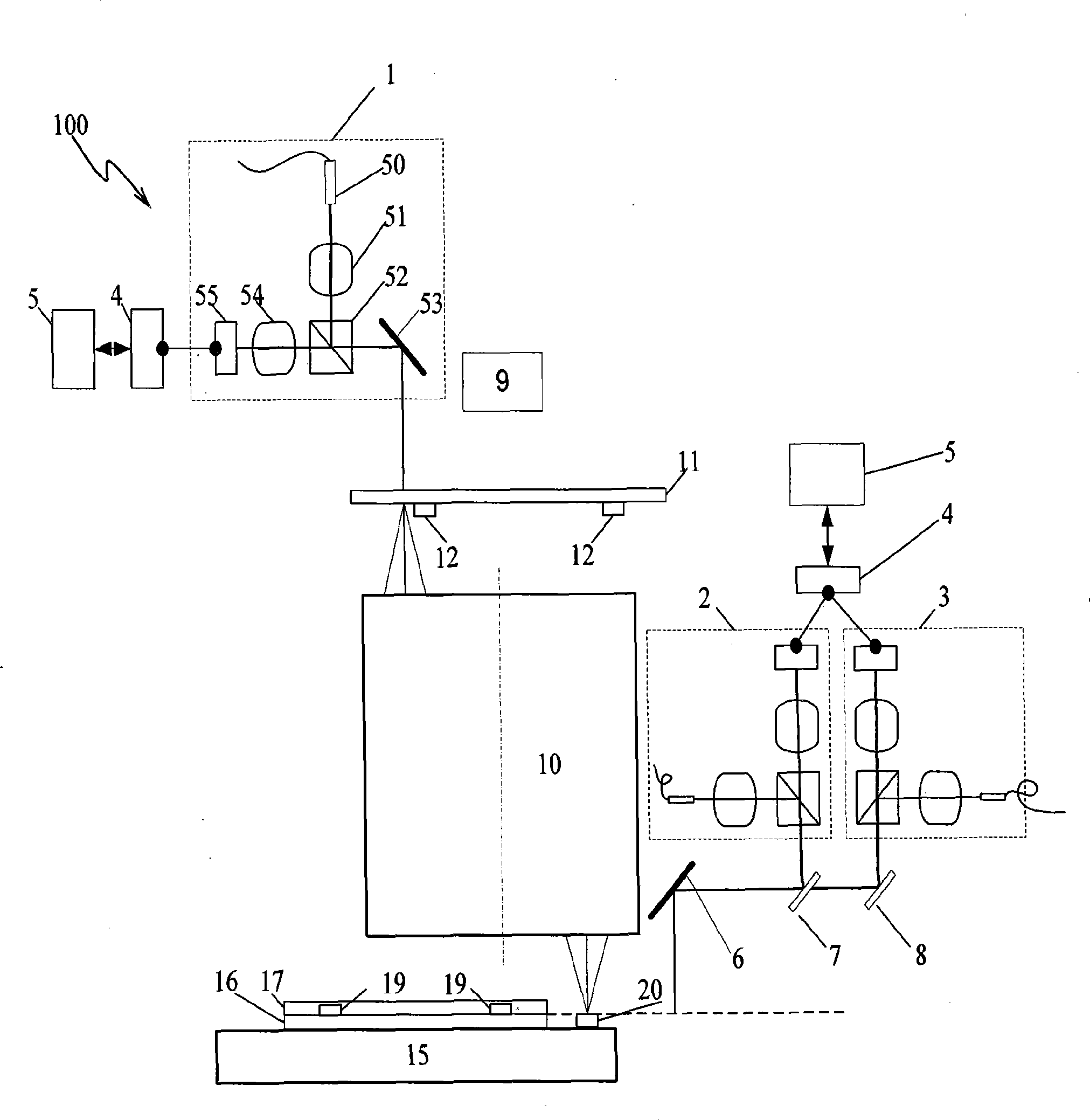
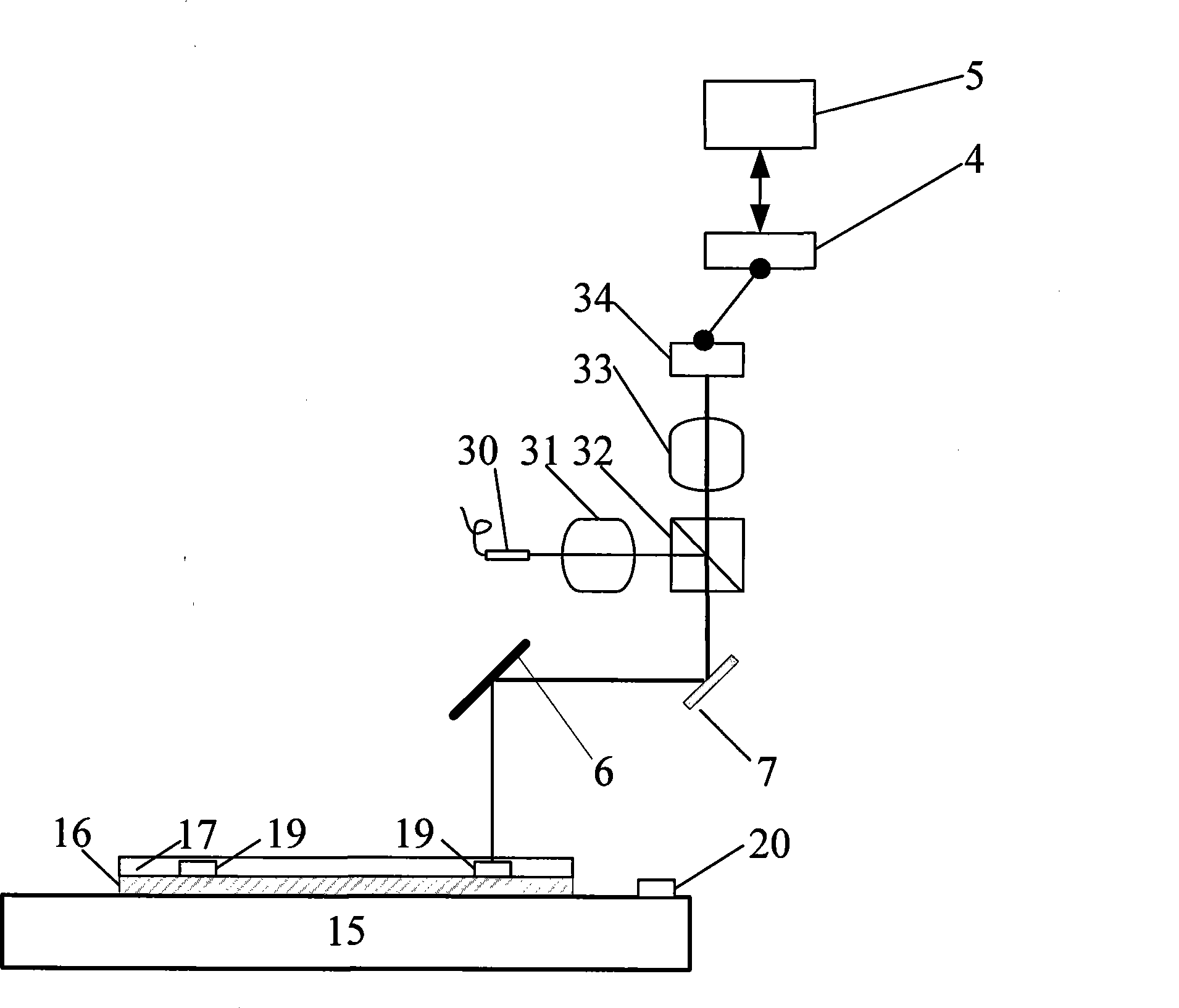
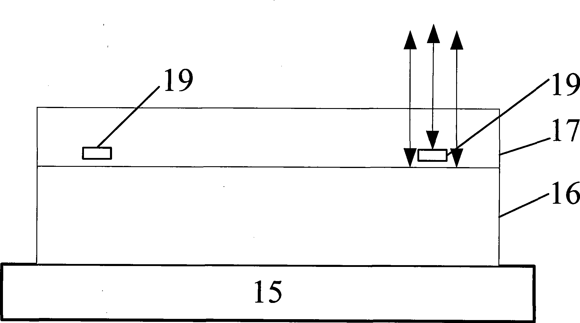
[0035] figure 1 Shown is a schematic diagram of a double-sided position alignment device according to an embodiment of the present invention. figure 2 Shown is a schematic diagram of the imaging principle of the first position alignment mark of the double-sided position alignment device according to an embodiment of the present invention. image 3 Shown is an optical path diagram of visible light irradiating the first position alignment mark according to an embodiment of the present invention. Figure 4 Shown is a schematic diagram of the imaging principle of the second position alignment mark of the double-sided position alignment device according to an embodiment of the present invention. Figure 5 Shown is an optical path diagram of infrared light irradiating the second position alignment mark according to an embodiment of the present invention.

[0036] Please refer to Figure 1 to Figure 5, The double-sided position alignment device 100 includes a mask 11, an optical projec...


PUM


Abstract

The invention provides a double-side position aligning device and a double-side position aligning method. The double-side position aligning device comprises a mask plate provided with a mask aligning mark, a work piece table provided with a reference aligning mark, a silicon chip illuminating system and an optical projecting system, and also comprises a mask position aligning device, an exposure object, a first side position aligning device, a second side position aligning device, an image collecting and processing system, and a control system, wherein the mask plate is horizontally arranged. The double-side position aligning device and the method can complex structural design and assembly of the exposure object and the work piece table, and can also improve technological adaptability of a back position aligning device for a silicon chip to a back aligning mark of the silicon chip.

Description

technical field [0001] The present invention relates to a double-sided position alignment device and method, and in particular to a double-sided position alignment device and method utilizing an ultraviolet illumination optical system, a visible light illumination optical system and an infrared illumination optical system. Background technique [0002] With the continuous improvement of people's living standards and the development of semiconductor technology, the semiconductor market will continue to increase the requirements for the intelligence and miniaturization of semiconductor packaging devices in the future. Digital products such as cameras, mobile phones, and PDAs are not only required to be small and easy to carry. It is also required to have multiple functions and low cost performance. In order to realize the development requirements of intelligence and miniaturization of packaged devices, there is a need for a multi-chip (silicon chip) package solution. Multi-di...

Claims


Application Information

Patent Timeline
IPC IPC(8): G03F9/00G03F7/20
Inventor 徐兵吕晓薇周畅李志丹
Owner SHANGHAI MICRO ELECTRONICS EQUIP (GRP) CO LTD
Why Eureka
Try Eureka