Eureka AIR delivers breakthrough ideas for toughest innovation challenges, trusted by R&D personnel around the world.

Plane double diffusion metal oxide semiconductor device and preparation method

An oxide semiconductor and double-diffusion technology, which is applied in semiconductor/solid-state device manufacturing, semiconductor devices, electrical components, etc., can solve the problems of large Rdson of PlanarDMOS devices, affecting the performance of PlanarDMOS devices, and high resistivity of the "neck" to reduce the Effects of Rjfet, channel widening, and width reduction

Active Publication Date: 2010-11-03
FOUNDER MICROELECTRONICS INT
View PDF0 Cites 0 Cited by
  • Summary
  • Abstract
  • Description
  • Claims
  • Application Information

AI Technical Summary

Problems solved by technology

[0004] The existing process for making Planar DMOS is to directly make Planar DMOS devices on the epitaxial layer of the wafer. Using this method to make Planar DMOS devices makes the die in the When it is turned on, the width of the depletion layer (width1) is relatively large, and the "neck" (width2) of the current channel is relatively narrow, so that the resistivity of the "neck" is relatively high, so Rjfet is relatively large, which in turn leads to Planar DMOS devices Rdson is large, which affects the performance of Planar DMOS devices

Method used


Image

  • Plane double diffusion metal oxide semiconductor device and preparation method
  • Plane double diffusion metal oxide semiconductor device and preparation method
  • Plane double diffusion metal oxide semiconductor device and preparation method

Examples


Embodiment Construction

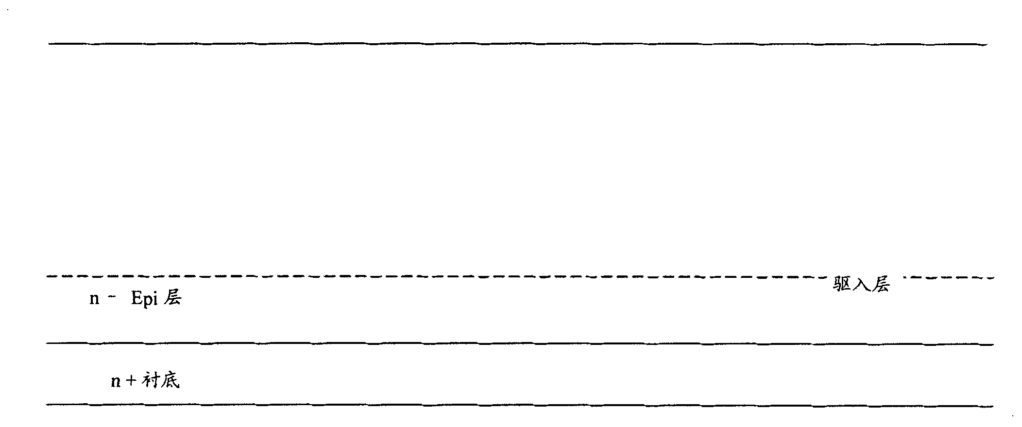
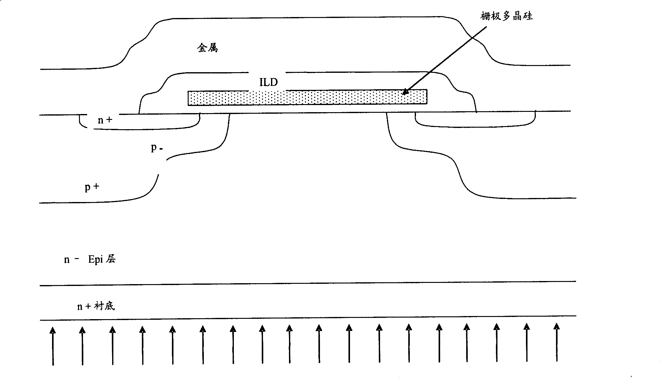
[0023] S201. Implanting first dopant atoms into the surface layer of the epitaxial layer of the wafer, so that the doping concentration of the surface layer of the epitaxial layer is higher than that of other parts of the epitaxial layer (see image 3 ).

[0024] Wherein, the wafer may be a silicon wafer, or a wafer made of other semiconductor materials.

[0025] The first dopant atoms include phosphorus atoms.

[0026] The method for implanting the first dopant atoms into the surface layer of the wafer epitaxial layer includes: placing the wafer epitaxial layer at one end of the ion implanter, and placing the doping source at the other end of the ion implanter. At one end of the dopant source, the first dopant atoms are ionized (with a certain charge), applied at an ultra-high speed by an electric field, and enter the surface layer of the epitaxial layer of the wafer.

[0027] refer to Figure 4 As shown, the purpose of injecting the first dopant atoms into the surface lay...


PUM


Abstract

The invention discloses a planar double-diffused metal oxide semiconductor device and a manufacturing method thereof, which aim to reduce on-resistance of a junction type field effect transistor of the planar double-diffused metal oxide semiconductor device and to increase the performance of the planar double-diffused metal oxide semiconductor. Before manufacturing a Planar DMOS device, the technical scheme includes implanting first doping atoms into the surface layer of a wafer epitaxial layer with doping concentration higher than that of another part of the epitaxial layer, driving the first doping atoms into the epitaxial layer for reducing resistivity of certain depth of the wafer epitaxial layer, thereby reducing the width of a deletion layer, widening the current passage, reducing the on-resistance of the junction type field effect transistor, further reducing the on-resistance and improving the performance of the planar double-diffused metal oxide semiconductor device.

Description

technical field [0001] The invention relates to the technical field of semiconductors, in particular to a manufacturing technology of a planar double-diffused metal oxide semiconductor device. Background technique [0002] A double diffused MOS (DMOS) is a metal oxide semiconductor field effect transistor (Metal Oxide Semiconductor Field Effect Transistor, MOSFET), which uses diffusion to form its transistor region. Double-diffused transistors are generally used as power transistors in high-voltage power integrated circuits to provide higher current per unit area under the requirement of low forward voltage drop. [0003] One type of double-diffused transistor is Planar DMOS (Planar Double-diffused MetalOxide Semiconductor, planar double-diffused metal oxide semiconductor), such as figure 1 As shown, in the PlanarDMOS process, Rdson=Rch+Ra+Rjfet+Repi+Rsub+Rc. Among them, Rdson is the on-resistance (static drain-source on-resistance), Rch is the channel resistance (channel ...

Claims


Application Information

Patent Timeline
Patent Type & Authority Patents(China)
IPC IPC(8): H01L21/336H01L21/265H01L29/36H01L29/78
Inventor 陈洪宁方绍明刘鹏飞王心强陈勇
Owner FOUNDER MICROELECTRONICS INT
Why Eureka
Eureka Blog
Learn More