Method for manufacturing film LED chip device based on gapless plane bonding

A device manufacturing method and LED chip technology, which is applied to semiconductor devices, electrical components, circuits, etc., can solve problems such as low yield rate and poor quality of permanent substrate bonding, so as to improve production efficiency, ensure film retention quality, The effect of ensuring the quality of workmanship

Active Publication Date: 2009-06-24
XIAMEN SANAN OPTOELECTRONICS TECH CO LTD
View PDF0 Cites 17 Cited by
  • Summary
  • Abstract
  • Description
  • Claims
  • Application Information

AI Technical Summary

Problems solved by technology

[0003] In order to solve the problems of poor bonding quality and low yield of the above-mentioned metal bonding (and electroplating) permanent substrates, the present invention aims to propose a thin-film LED chip device manufacturing method based on seamless planar bonding

Method used


Image

  • Method for manufacturing film LED chip device based on gapless plane bonding
  • Method for manufacturing film LED chip device based on gapless plane bonding
  • Method for manufacturing film LED chip device based on gapless plane bonding

Examples


Embodiment Construction

[0022] The present invention will be further described below in conjunction with the accompanying drawings and embodiments.

[0023] A method for manufacturing a thin-film LED chip device based on seamless planar bonding, the steps of which are:

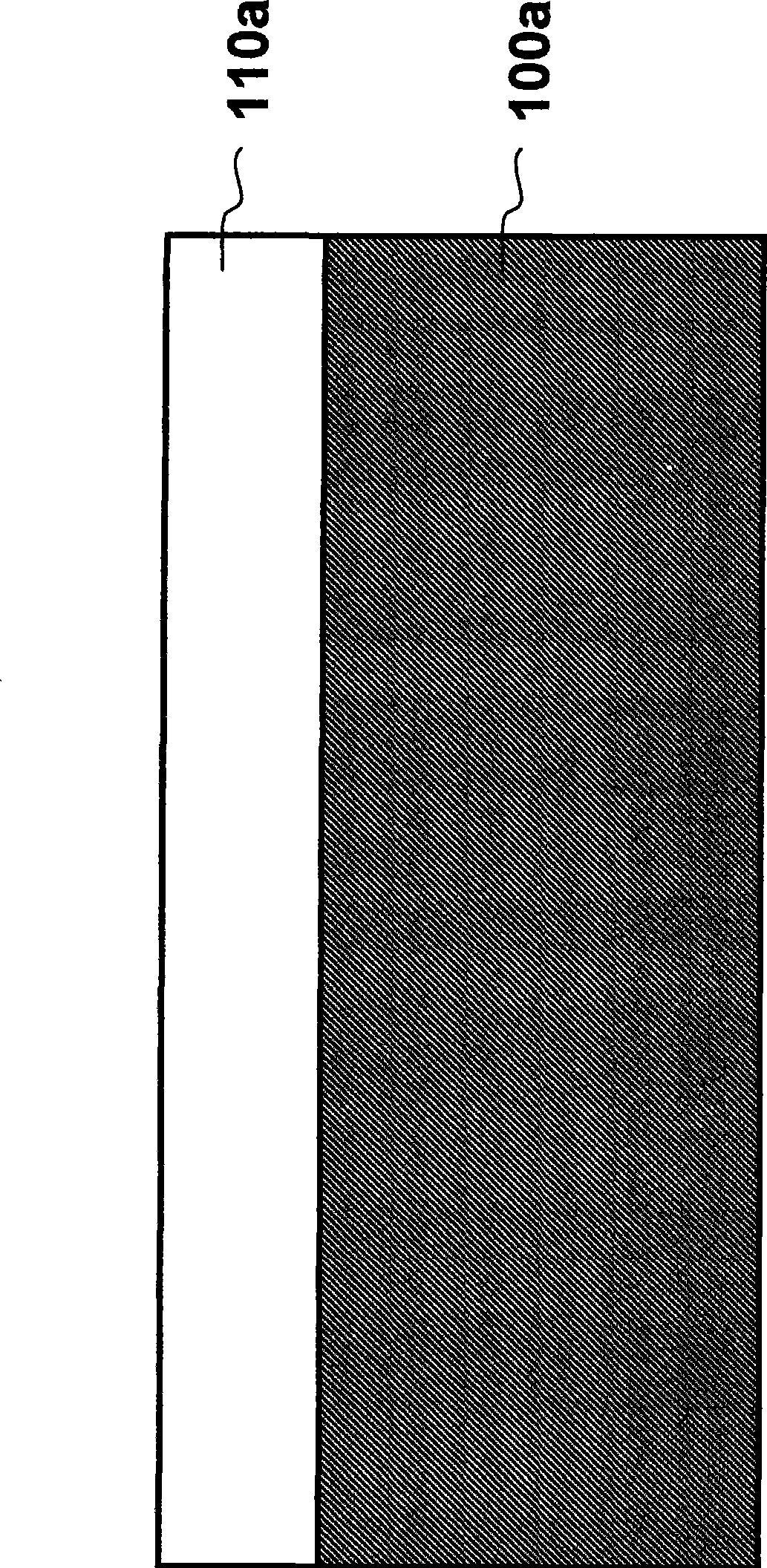
[0024] Step 1: First, if Figure 1a As shown, a nitride semiconductor epitaxial film 110a is heteroepitaxially grown on a sapphire substrate 100a, and the epitaxial film 110a has an N-GaN layer, an active layer, and a P-GaN layer.

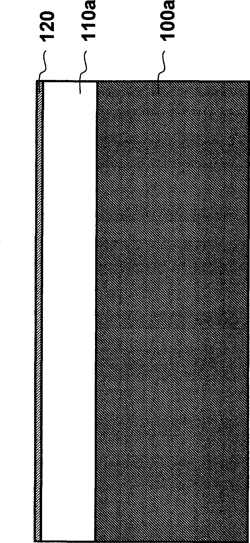
[0025] Step 2: If Figure 1b . As shown, an ohmic contact and a metal reflective adhesive layer 120 are formed on the top of the above-mentioned epitaxial film 110a. The material of the metal reflective layer is firstly Ag, with a thickness of 50-500nm. It can also be made of Al, Ag, Ni, Au, Cu, Pd and It is made of an alloy formed by two or more substances in the Rh composition material group, and is made of N 2 High-temperature annealing in the atmosphere to achieve ohmic contact characteristics and e...


PUM


Abstract

The invention discloses a preparation method of a film LED chip device based on the gapless plane bonding; the method makes use of the smooth surface of an epitaxial wafer without isolated processing to prepare a permanent or temporary substrate; then laser beams are used for unit isolated processing of devices at the interface position between the epitaxial layer and the substrate so as to ensure the combination yield rate of the substrate and the epitaxial layer, thereby ensuring the film-remaining yield rate of the epitaxial thin film layer after laser stripping and also simplifying the traditional production process.

Description

technical field [0001] The invention relates to a light-emitting diode chip manufacturing process, in particular to a thin-film LED chip device manufacturing method based on seamless plane bonding. Background technique [0002] In order to improve the luminous performance of LED chip devices, excimer laser stripping sapphire technology has gradually been recognized and used by the LED manufacturing industry. However, the quality of the epitaxial layer remaining after sapphire stripping has always been a key issue for LED manufacturers. . The conventional process is to first isolate the GaN epitaxial wafer for device cycles, then perform metal bonding or electroplating on a permanent (or temporary) substrate, and then perform excimer laser lift-off on the sapphire substrate used to grow the GaN epitaxial layer to obtain the remaining GaN epitaxial thin films on permanent (or temporary) temporary substrates, but the film quality of existing traditional processes needs to be i...

Claims


Application Information

Patent Timeline
Patent Type & Authority Applications(China)
IPC IPC(8): H01L33/00
Inventor 陈文欣林雪娇潘群峰吴志强洪灵愿
Owner XIAMEN SANAN OPTOELECTRONICS TECH CO LTD
Why Eureka
Try Eureka