

Non-contact type embedded body of electronic credential and method for producing the same
A non-contact, electronic certificate technology, applied to record carriers, computer parts, printing, etc. used by machines, can solve the problems of unsuitable certificate cover, lack of extensiveness, single material selection, etc., and achieve simple manufacturing methods, The effect of strong firmness and reduction of manufacturing cost
- Summary
- Abstract
- Description
- Claims
- Application Information
AI Technical Summary
Problems solved by technology
Method used
Image

Examples
example 1
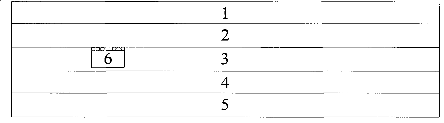
[0036] refer to figure 1 In the structure shown, materials for the upper protective layer 1 , the upper connection layer 2 , the chip carrier layer 3 , the lower connection layer 4 , and the lower protective layer 5 are prepared. The upper protective layer 1 and the lower protective layer 5 use soft materials that are suitable for the document binding process and have a strong bonding force with traditional paper adhesives. The die-cutting of the chip hole is carried out on the chip carrying layer 3 , and then the embedding work of the non-contact coil and the chip 6 is carried out on the chip carrying layer 3 . In this example, the chip carrier layer 3 preferably has a thickness of 0.15-0.25mm, the upper connection layer 2 and the lower connection layer 4 have a thickness of 0.04-0.06mm, and the upper protective layer and the lower protective layer both have a thickness of 0.12-0.15mm. After all the materials are prepared, the figure 1 After the stacking is completed, lam...
example 2
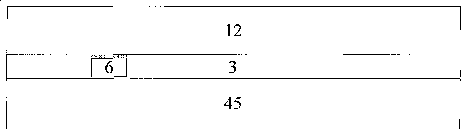
[0038] like figure 2 As shown, the upper protective layer 1 and the upper connecting layer 2, the lower connecting layer 4 and the lower protective layer 5 are pre-compounded to obtain an upper composite fabric 12 and a lower composite fabric 45 with a thickness of 0.1 mm to 0.2 mm. The composite method can use high temperature thermal composite method, tape casting method to directly composite, or use adhesive bonding method, after bonding, perform high temperature and high pressure operation as described in Example 1, and finally make it as figure 2 Finished contactless insert shown.
example 3
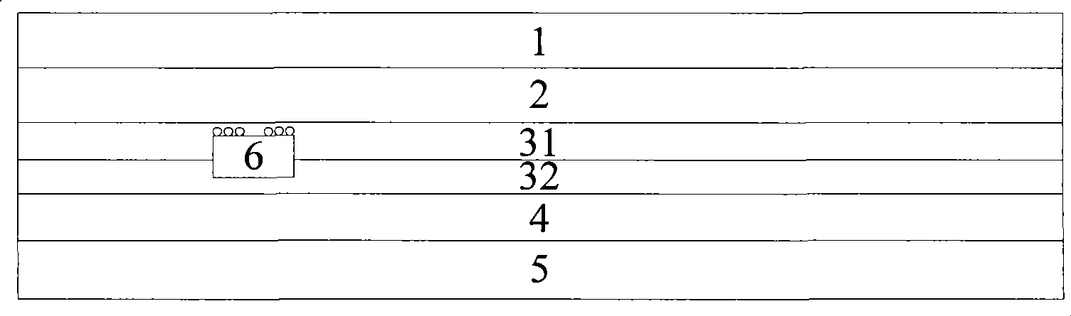
[0040] like image 3As shown, when making a non-contact embedded body, adjust the structure of the non-contact embedded body according to the structure of the chip, such as adjusting the chip carrier layer 3 to a two-layer structure of the first layer structure 31 and the second layer structure 32, so as to Adapt to the thickness of the chip. For example, the thickness of the first layer structure 31 is 0.1mm, and the thickness of the second layer structure 32 is 0.15mm, and then according to the operation of Example 1, it is finally made as image 3 Finished touchless insert shown.
PUM
| Property | Measurement | Unit |
|---|---|---|
| Thickness | aaaaa | aaaaa |
| Thickness | aaaaa | aaaaa |
| Thickness | aaaaa | aaaaa |
Abstract
Description
Claims
Application Information