Method for extension of plumbago alkene with ultra-thin hexagonal phase silicon carbide membrane on insulated substrate

A technology of silicon carbide film on insulating substrate, applied in the field of semiconductor low-dimensional thin film material preparation, can solve the problems of restricting the performance of graphene devices and high cost of epitaxial graphene

Inactive Publication Date: 2009-07-29
INST OF SEMICONDUCTORS - CHINESE ACAD OF SCI
View PDF0 Cites 24 Cited by
  • Summary
  • Abstract
  • Description
  • Claims
  • Application Information

AI Technical Summary

Problems solved by technology

However, the latter method uses an expensive silicon carbide semi-insulating substrate, which makes the cost of epitaxial graphene too high. In addition, the interaction between the silicon carbide substrate and graphene restricts the device performance of graphene ( F. Varchon, Physical Review Letters, 2007)

Method used


Image

  • Method for extension of plumbago alkene with ultra-thin hexagonal phase silicon carbide membrane on insulated substrate
  • Method for extension of plumbago alkene with ultra-thin hexagonal phase silicon carbide membrane on insulated substrate
  • Method for extension of plumbago alkene with ultra-thin hexagonal phase silicon carbide membrane on insulated substrate

Examples


Embodiment 1

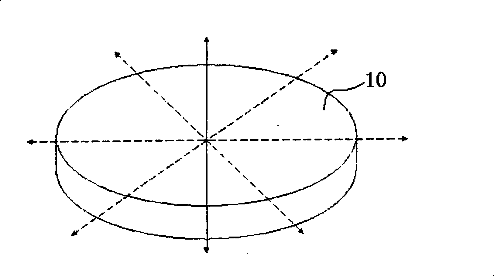
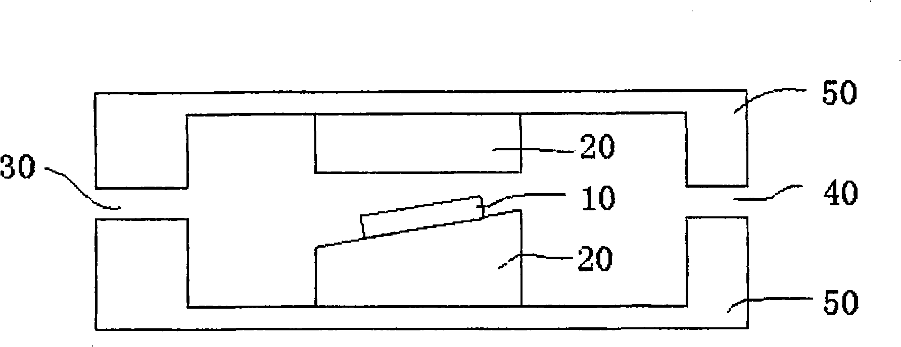
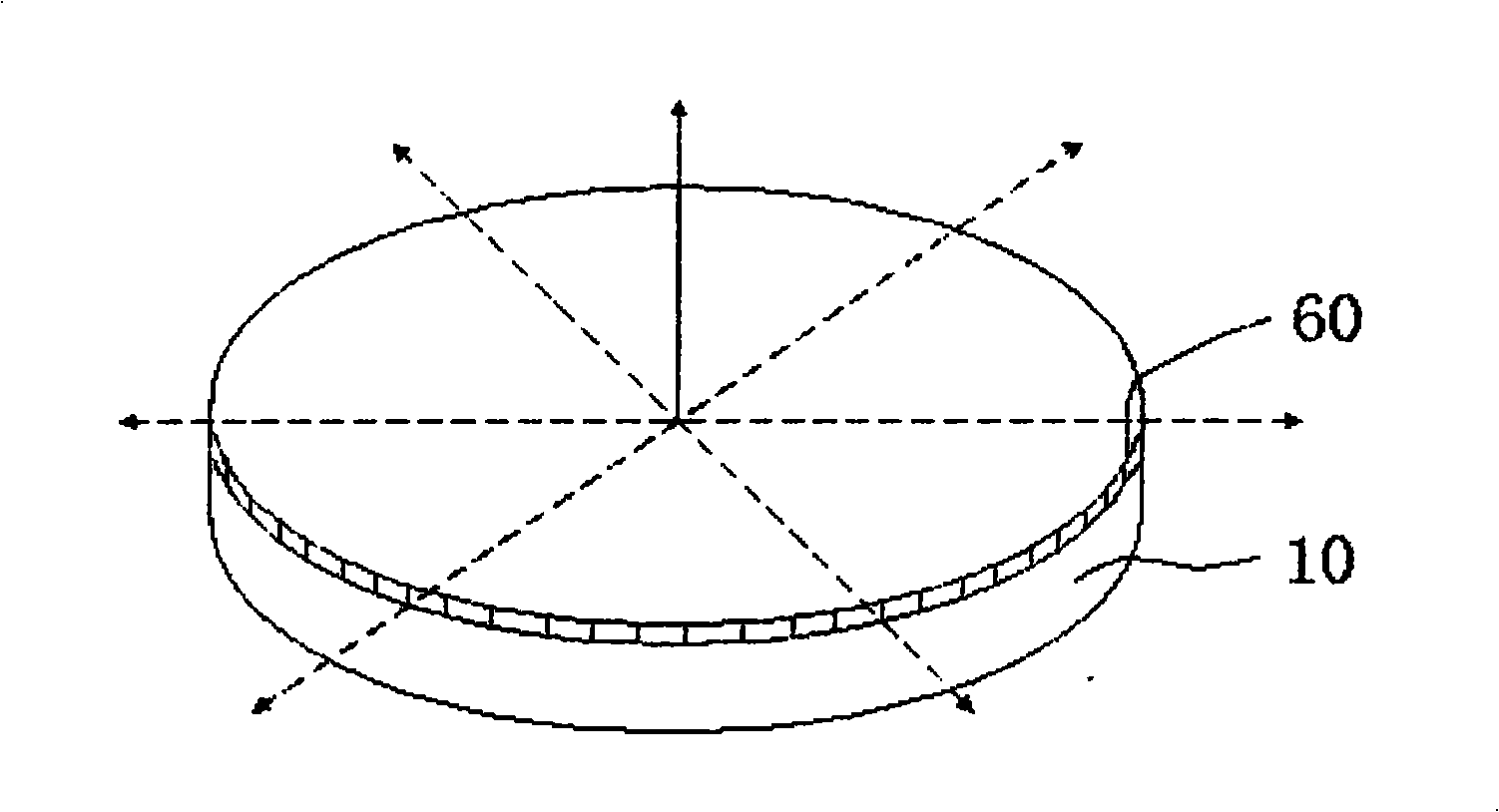
[0050] Single crystal sapphire substrate (α-Al 2 o 3 ) (insulating substrate 10), the surface of C (0001) is chemically polished, cleaned and placed in a growth furnace, and hydrogen gas is introduced to etch and polish the surface of the single crystal sapphire substrate. The hydrogen flow rate during etching is 3000 sccm, The surface temperature of the single crystal sapphire substrate is 1350° C., the pressure in the growth chamber is normal pressure, and the etching is performed for 30 minutes. After etching, the surface of the substrate can be seen under the microscope to be flat at the atomic level, without defects such as scratches. Then feed ammonia gas to carry out nitriding treatment on the surface of the single crystal sapphire substrate. During nitriding, the flow rate of ammonia gas is 1 sccm, the surface temperature of the single crystal sapphire substrate is 1500° C., the growth chamber pressure is 40 Torr, and the nitriding treatment is carried out for 10 minu...


PUM


Abstract

The invention provides a method for preparing graphene by epitaxy of an ultrathin hexagonal phase silicon carbide film on an insulating substrate. The method is characterized by comprising the following steps: step one, taking the insulating substrate; step two, carrying out high-temperature etching pretreatement on the insulating substrate by hydrogen to remove surface scratch and other deficiencies so as to obtain flat surface; step three, carrying out high-temperature nitrogen treatment on the insulating substrate to activate the epitaxial surface so as to ensure that subsequent silicon carbide can be easily adhered on the surface of the substrate and maintain the same crystallographic orientation relationship with the substrate; step four, extending the hexagonal phase monocrystal silicon carbide on the insulating substrate; and step five, vaporizing silicon ions in the silicon carbide to complete preparation of the graphene on the insulating substrate.

Description

technical field [0001] The invention belongs to the field of semiconductor low-dimensional film material preparation, in particular to a method for epitaxial graphene from an ultra-thin hexagonal silicon carbide film on an insulating substrate. Background technique [0002] Graphene (Graphene) is a thin sheet composed of a single layer or several layers (less than 100 layers) of carbon atoms. Such a two-dimensional graphite sheet has been proved to have many super properties, such as its electrons in submicron distances Ballistic transportation, without any scattering, has a very attractive conductivity, which provides conditions for the manufacture of super-performance transistors. Graphene transistors can work at room temperature, and it is predicted that graphene films may eventually replace silicon, because graphene transistors are more efficient, faster and consume less energy than silicon tubes. [0003] Graphene has brought a new opportunity to the semiconductor indu...

Claims


Application Information

Patent Timeline
Patent Type & Authority Applications(China)
IPC IPC(8): C30B29/02C30B25/02
Inventor 刘兴昉孙国胜李晋闽赵永梅王雷赵万顺王亮纪刚杨挺曾一平
Owner INST OF SEMICONDUCTORS - CHINESE ACAD OF SCI
Why Eureka
Try Eureka