Conductive glass of dye-sensitized solar cell
A solar cell and conductive glass technology, applied in capacitor electrodes, circuits, photovoltaic power generation, etc., can solve the problems of long electron transmission distance, reduction of fill factor and photoelectric conversion efficiency, and lower photoelectric conversion efficiency
- Summary
- Abstract
- Description
- Claims
- Application Information
AI Technical Summary
Problems solved by technology
Method used
Image
Examples
Embodiment 1
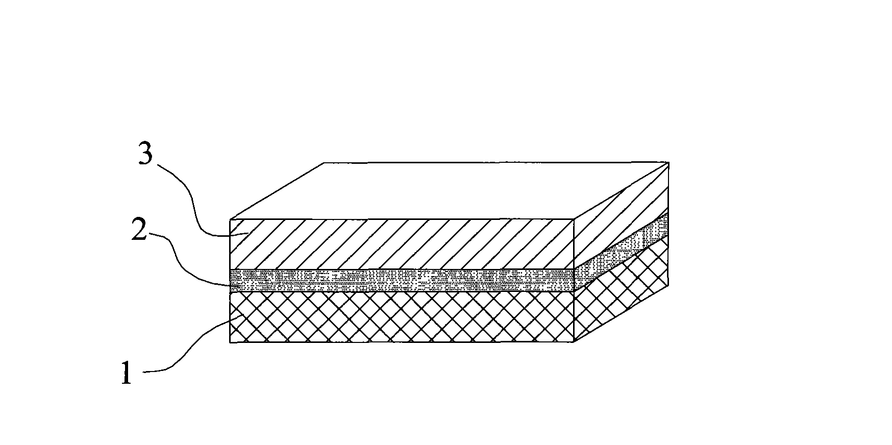
[0016] A conductive glass for a dye-sensitized solar cell, comprising a conductive glass layer and a titanium dioxide barrier film layer, characterized in that a low-resistance grid electrode is arranged between the conductive glass layer and the titanium dioxide barrier film layer, and the titanium dioxide barrier film layer will The low resistance gate electrode is isolated from the external environment.
[0017] Wherein: the conductive glass layer is FTO conductive glass.
[0018] Low-resistance grid electrode: using medium-temperature silver paste as material, it is printed on the upper surface of FTO glass at one time by screen printing method, and the low-resistance grid is printed into a mesh shape. The printing method is: use JG6080 screen printing machine, 300-mesh screen, and sinter at 450°C for half an hour after printing to make a low-resistance grid. The line width of the obtained low-resistance grid is 0.5mm.
[0019] Titanium dioxide barrier layer: dense titani...
Embodiment 2
[0021] A conductive glass for a dye-sensitized solar cell, comprising a conductive glass layer and a titanium dioxide barrier film layer, characterized in that a low-resistance grid electrode is arranged between the conductive glass layer and the titanium dioxide barrier film layer, and the titanium dioxide barrier film layer will The low resistance gate electrode is isolated from the external environment.
[0022] Wherein: the conductive glass layer is FTO conductive glass.
[0023] Low-resistance grid electrode: using medium-temperature silver paste as material, it is printed on the upper surface of the bottom plate FTO glass at one time by screen printing method, and the low-resistance grid is printed into a mesh shape. The printing method is: use JG6080 screen printing machine, 300-mesh screen, and sinter at 450°C for half an hour after printing to make a low-resistance grid. The line width of the obtained low-resistance grid is 0.5mm.
[0024] Titanium dioxide barrier fi...
Embodiment 3
[0026] A conductive glass for a dye-sensitized solar cell, comprising a conductive glass layer and a titanium dioxide barrier film layer, characterized in that a low-resistance grid electrode is arranged between the conductive glass layer and the titanium dioxide barrier film layer, and the titanium dioxide barrier film layer will The low resistance gate electrode is isolated from the external environment.
[0027] Wherein: the conductive glass layer is FTO conductive glass.
[0028] Low-resistance grid electrode: using medium-temperature silver paste as material, it is printed on the upper surface of the bottom plate FTO glass at one time by screen printing method, and the low-resistance grid is printed into a mesh shape. The printing method is: use JG6080 screen printing machine, 300-mesh screen, and sinter at 450°C for half an hour after printing to make a low-resistance grid. The line width of the obtained low-resistance grid is 0.5mm.
[0029] Titanium dioxide barrier fi...
PUM
| Property | Measurement | Unit |
|---|---|---|
| Line width | aaaaa | aaaaa |
Abstract
Description
Claims
Application Information
