Superficial treatment method of printed wiring board

A printed circuit board and surface treatment technology, which is applied in the direction of liquid chemical plating, metal material coating process, coating, etc., to achieve the effect of preventing oxidation and ensuring reliability

Active Publication Date: 2009-09-09
SHENZHEN CHENGGONG CHEM
View PDF0 Cites 71 Cited by
  • Summary
  • Abstract
  • Description
  • Claims
  • Application Information

AI Technical Summary

Problems solved by technology

Of these four finishes, none can meet all the needs of a lead-free assembly process, especially when multi

Method used


Image

  • Superficial treatment method of printed wiring board
  • Superficial treatment method of printed wiring board
  • Superficial treatment method of printed wiring board

Examples


example 1

[0046] Process parameters:

[0047]

[0048]

[0049] Main steps Material name and content:

[0050] product name

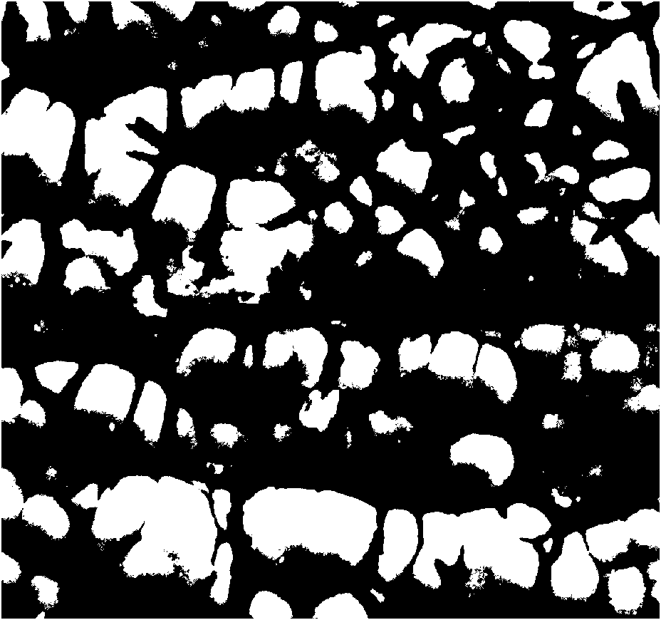
[0051] According to the above process, the appearance of the plated product is uniform, and the bonding strength between the metal layers meets the standard requirements. The thickness of nickel is 4.1um, the thickness of palladium is 0.092um, and the thickness of gold is 0.087um. It is used for SMT (surface mount technology) and Bonding performance test is good. After the gold is withdrawn from the finished product, observe the corrosion condition of the nickel surface, see image 3 , Figure 4 , The results show that there is no black disk phenomenon of nickel corrosion on the surface!

example 2

[0053] Process parameters:

[0054] steps

[0055] Main steps Material name and content:

[0056] product name

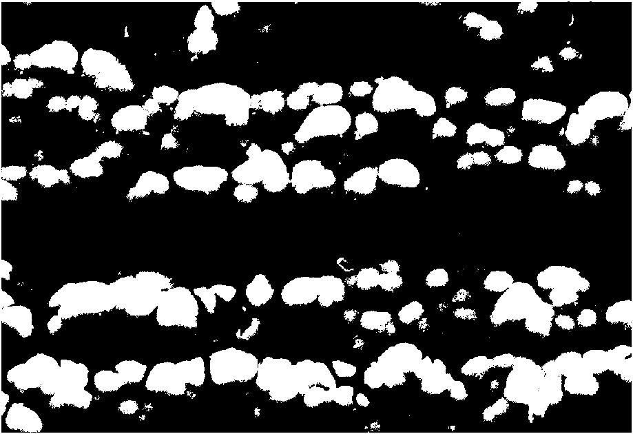
[0057] According to the above process, the appearance of the plated product is uniform, and the bonding strength between the metal layers meets the standard requirements. The thickness of nickel is 4.8um, the thickness of palladium is 0.086um, and the thickness of gold is 0.093um. It is made of SMT (surface mount technology) and Bonding performance test is good. After the gold is withdrawn from the finished product, observe the corrosion condition of the nickel surface, see Figure 5 , Image 6 , The results show that there is no black disk phenomenon of nickel corrosion on the surface!

example 3

[0059] Process parameters:

[0060]

[0061]

[0062] Main steps Material name and content:

[0063]

[0064]

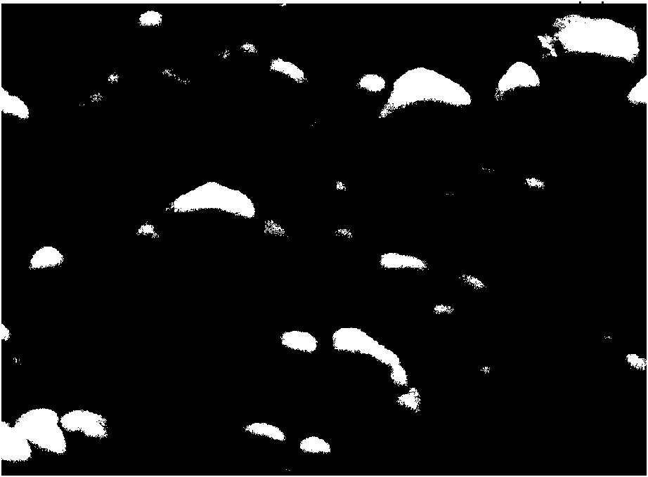
[0065] According to the above process, the appearance of the plated product is uniform, and the bonding strength between the metal layers meets the standard requirements. The thickness of nickel is 4.2um, the thickness of palladium is 0.090um, and the thickness of gold is 0.079um. It is used for SMT (surface mount technology) and Bonding performance test is good. After the gold is withdrawn from the finished product, observe the corrosion condition of the nickel surface, see Figure 7 , Figure 8 , The results show that there is no black disk phenomenon of nickel corrosion on the surface!

[0066] Process characteristics of the present invention: 1. The acidic cleaner is aimed at thin lines, small aperture high-precision circuit boards, has good cleaning power, will not attack the solder resist ink of the circuit board, can strongly remove the oxidatio...


PUM

PropertyMeasurementUnit
Thicknessaaaaaaaaaa
Thicknessaaaaaaaaaa
Thicknessaaaaaaaaaa

Abstract

The invention discloses a superficial treatment method of printed wiring board, which is dedicated to solving the technical problem of preventing black pad in the process of plating ENIG by chemical means, ensuring reliability of welding and routing process. The method comprises the following steps: chemical Immersion of nickel, chemical immersion of palladium and chemical gilding. Compared with the prior art, chemical immersion of nickel, chemical immersion of palladium and chemical gilding are carried out on the printed wiring board to obtain Ni/Pd gold plating, thus effectively preventing long-term oxidization of palladium surface in the air and ensuring reliability of welding combination and routing combination.

Description

technical field [0001] The invention relates to a method for manufacturing a printed circuit board, in particular to a surface treatment method for a printed circuit board. Background technique [0002] In recent years, the development of electronic products has been very rapid, and the PCB manufacturing industry of printed circuit boards has also increased accordingly. Surface mount SMT technology has developed steadily and rapidly in our country. Driven by the trend of lead-free, the surface treatment method of printed circuit boards The requirements are getting higher and higher, and the application volume of integrated circuit IC substrates has also increased significantly. The surface treatment methods of printed circuit boards in the prior art are: chemical immersion nickel gold, electroplating nickel gold, chemical immersion tin, chemical immersion silver, OSP process, or spray tin. The advantages and disadvantages of these six processes are very prominent; chemical i...

Claims


Application Information

Patent Timeline
IPC IPC(8): C23C18/31C23C18/36C23C18/44
Inventor 姚成
Owner SHENZHEN CHENGGONG CHEM
Why Eureka
Try Eureka